- 您現在的位置:買賣IC網 > PDF目錄373920 > AD7854L (Analog Devices, Inc.) 12-Bit Sampling ADC(單電源,200kSPS 12位采樣A/D轉換器) PDF資料下載
參數資料
| 型號: | AD7854L |
| 廠商: | Analog Devices, Inc. |
| 英文描述: | 12-Bit Sampling ADC(單電源,200kSPS 12位采樣A/D轉換器) |
| 中文描述: | 12位采樣ADC(單電源,速度高達200ksps的12位采樣的A / D轉換器) |
| 文件頁數: | 5/28頁 |
| 文件大小: | 268K |
| 代理商: | AD7854L |
第1頁第2頁第3頁第4頁當前第5頁第6頁第7頁第8頁第9頁第10頁第11頁第12頁第13頁第14頁第15頁第16頁第17頁第18頁第19頁第20頁第21頁第22頁第23頁第24頁第25頁第26頁第27頁第28頁
AD7854/AD7854L
REV. 0
–5–
ORDE RING GUIDE
Linearity
E rror
(LSB)
Power
Dissipation
(mW)
T emperature
Range
1
Package
Option
2
Model
AD7854AQ
AD7854SQ
AD7854AR
AD7854BR
AD7854ARS
AD7854LAR
3
AD7854LBR
3
AD7854LARS
3
EVAL-AD7854CB
4
EVAL-CONT ROL BOARD
5
–40
°
C to +85
°
C
–55
°
C to +125
°
C
–40
°
C to +85
°
C
–40
°
C to +85
°
C
–40
°
C to +85
°
C
–40
°
C to +85
°
C
–40
°
C to +85
°
C
–40
°
C to +85
°
C
1
1
1
1/2
1
1
1/2
1
15
15
15
15
15
15
15
5.5
Q-28
Q-28
R-28
R-28
RS-28
R-28
R-28
RS-28
NOT ES
1
Linearity error refers to the integral linearity error.
2
Q = Cerdip; R = SOIC; RS = SSOP.
3
L signifies the low power version.
4
T his can be used as a stand-alone evaluation board or in conjunction with the EVAL-CONT ROL BOARD for
evaluation/demonstration purposes.
5
T his board is a complete unit allowing a PC to control and communicate with all Analog Devices evaluation boards
ending in the CB designator. For more information on Analog Devices products and evaluation boards visit our
World Wide Web home page at http://www.analog.com.
TO
OUTPUT
PIN
+2.1V
I
OH
1.6mA
200μA
I
OL
C
L
50pF
Figure 1. Load Circuit for Digital Output Timing
Specifications
ABSOLUT E MAX IMUM RAT INGS
1
(T
A
= +25
°
C unless otherwise noted)
AV
DD
to AGND . . . . . . . . . . . . . . . . . . . . . . . . –0.3 V to +7 V
DV
DD
to DGND . . . . . . . . . . . . . . . . . . . . . . . –0.3 V to +7 V
AV
DD
to DV
DD
. . . . . . . . . . . . . . . . . . . . . . . –0.3 V to +0.3 V
Analog Input Voltage to AGND . . . . –0.3 V to AV
DD
+ 0.3 V
Digital Input Voltage to DGND . . . . –0.3 V to DV
DD
+ 0.3 V
Digital Output Voltage to DGND . . . –0.3 V to DV
DD
+ 0.3 V
REF
IN
/REF
OUT
to AGND . . . . . . . . . –0.3 V to AV
DD
+ 0.3 V
Input Current to Any Pin Except Supplies
2
. . . . . . . .
±
10 mA
Operating T emperature Range
Commercial (A, B Versions) . . . . . . . . . . . –40
°
C to +85
°
C
Commercial (S Version) . . . . . . . . . . . . . . –55
°
C to +125
°
C
Storage T emperature Range . . . . . . . . . . . –65
°
C to +150
°
C
Junction T emperature . . . . . . . . . . . . . . . . . . . . . . . . . +150
°
C
Cerdip Package, Power Dissipation . . . . . . . . . . . . . . 450 mW
θ
JA
T hermal Impedance . . . . . . . . . . . . . . . . . . . . . . 75
°
C/W
Lead T emperature, (Soldering, 10 secs) . . . . . . . . . . +300
°
C
SOIC, SSOP Package, Power Dissipation . . . . . . . . . 450 mW
θ
JA
T hermal Impedance . . . 75
°
C/W (SOIC) 115
°
C/W (SSOP)
θ
JC
T hermal Impedance . . . 25
°
C/W (SOIC) 35
°
C/W (SSOP)
Lead T emperature, Soldering
Vapor Phase (60 secs) . . . . . . . . . . . . . . . . . . . . . . +215
°
C
Infrared (15 secs) . . . . . . . . . . . . . . . . . . . . . . . . . +220
°
C
NOT ES
1
Stresses above those listed under “Absolute Maximum Ratings” may cause
permanent damage to the device. T his is a stress rating only and functional
operation of the device at these or any other conditions above those listed in the
operational sections of this specification is not implied. Exposure to absolute
maximum rating conditions for extended periods may affect device reliability.
2
T ransient currents of up to 100 mA will not cause SCR latchup.
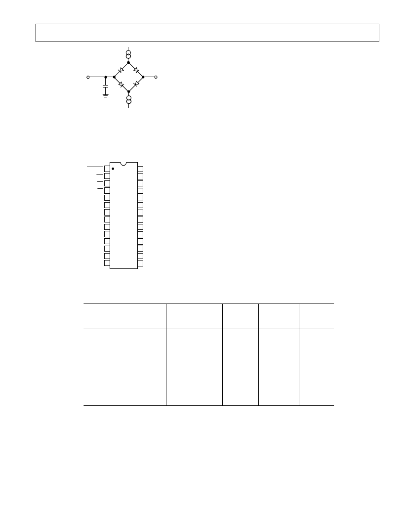
PIN CONFIGURAT ION
FOR DIP, SOIC AND SSOP
14
13
12
11
17
16
15
20
19
18
10
9
8
1
2
3
4
7
6
5
TOP VIEW
(Not to Scale)
28
27
26
25
24
23
22
21
AD7854
CONVST
DB10
DB11
CLKIN
BUSY
WR
RD
CS
DV
DD
DB8
DGND
DB9
REF
IN
/REF
OUT
AV
DD
AGND
C
REF1
C
REF2
AIN(+)
DB6
DB7
AIN(–)
HBEN
DB0
DB1
DB5
DB2
DB3
DB4
相關PDF資料 |
PDF描述 |
|---|---|
| AD7854 | 12-Bit Sampling ADC(單電源,200kSPS 12位采樣A/D轉換器) |
| AD7858LARS | 3 V to 5 V Single Supply, 200 kSPS 8-Channel, 12-Bit Sampling ADC |
| AD7858BN | 3 V to 5 V Single Supply, 200 kSPS 8-Channel, 12-Bit Sampling ADC |
| AD7858BR | 3 V to 5 V Single Supply, 200 kSPS 8-Channel, 12-Bit Sampling ADC |
| AD7858AN | 3 V to 5 V Single Supply, 200 kSPS 8-Channel, 12-Bit Sampling ADC |
相關代理商/技術參數 |
參數描述 |
|---|---|
| AD7854LAQ | 制造商:Rochester Electronics LLC 功能描述:12 BIT SINGLE CHANNEL PARALLEL ADC I.C. - Bulk |
| AD7854LAR | 制造商:Analog Devices 功能描述:ADC Single SAR 100ksps 12-bit Parallel 28-Pin SOIC W 制造商:Rochester Electronics LLC 功能描述:12-BIT SINGLE CHANNEL PARALLEL ADC I.C. - Bulk |
| AD7854LAR-REEL | 制造商:Analog Devices 功能描述:ADC Single SAR 100ksps 12-bit Parallel 28-Pin SOIC W T/R 制造商:Analog Devices 功能描述:ADC SGL SAR 100KSPS 12-BIT PARALLEL 28SOIC W - Tape and Reel |
| AD7854LARS | 功能描述:IC ADC 12BIT PARALLEL LP 28-SSOP RoHS:否 類別:集成電路 (IC) >> 數據采集 - 模數轉換器 系列:- 產品培訓模塊:Lead (SnPb) Finish for COTS Obsolescence Mitigation Program 標準包裝:2,500 系列:- 位數:12 采樣率(每秒):3M 數據接口:- 轉換器數目:- 功率耗散(最大):- 電壓電源:- 工作溫度:- 安裝類型:表面貼裝 封裝/外殼:SOT-23-6 供應商設備封裝:SOT-23-6 包裝:帶卷 (TR) 輸入數目和類型:- |
發布緊急采購,3分鐘左右您將得到回復。