- 您現(xiàn)在的位置:買賣IC網(wǎng) > PDF目錄373969 > AD9866CHIPS (ANALOG DEVICES INC) Broadband Modem Mixed Signal Front End PDF資料下載
參數(shù)資料
| 型號(hào): | AD9866CHIPS |
| 廠商: | ANALOG DEVICES INC |
| 元件分類: | 通信及網(wǎng)絡(luò) |
| 英文描述: | Broadband Modem Mixed Signal Front End |
| 中文描述: | SPECIALTY TELECOM CIRCUIT, UUC |
| 文件頁(yè)數(shù): | 36/48頁(yè) |
| 文件大小: | 1647K |
| 代理商: | AD9866CHIPS |
第1頁(yè)第2頁(yè)第3頁(yè)第4頁(yè)第5頁(yè)第6頁(yè)第7頁(yè)第8頁(yè)第9頁(yè)第10頁(yè)第11頁(yè)第12頁(yè)第13頁(yè)第14頁(yè)第15頁(yè)第16頁(yè)第17頁(yè)第18頁(yè)第19頁(yè)第20頁(yè)第21頁(yè)第22頁(yè)第23頁(yè)第24頁(yè)第25頁(yè)第26頁(yè)第27頁(yè)第28頁(yè)第29頁(yè)第30頁(yè)第31頁(yè)第32頁(yè)第33頁(yè)第34頁(yè)第35頁(yè)當(dāng)前第36頁(yè)第37頁(yè)第38頁(yè)第39頁(yè)第40頁(yè)第41頁(yè)第42頁(yè)第43頁(yè)第44頁(yè)第45頁(yè)第46頁(yè)第47頁(yè)第48頁(yè)
AD9866
Rev. 0 | Page 36 of 48
0
1.0V
TO
ADCs
REFT
REFB
C1
0.1
μ
F
C2
10
μ
F
C3
0.1
μ
F
C4
μ
F
C1
C4
C2
C3
TOP
VIEW
AGC TIMING CONSIDERATIONS
When implementing a digital AGC timing loop, it is important
to consider the Rx path latency and settling time of the Rx path
in response to a change in gain setting. Figure 21 and Figure 24
show the RxPGA’s settling response to a 60 dB and 5 dB change
in gain setting when using the Tx[5:0] or PGA[5:0] port. While
the RxPGA settling time may also show a slight dependency on
the LPF’s cutoff frequency, the ADC’s pipeline delay along with
the ADIO bus interface presents a more significant delay. The
amount of delay or latency depends on whether a half- or full-
duplex is selected. An impulse response at the RxPGA’s input
can be observed after 10.0 ADC clock cycles (1/f
ADC
) in the case
of a half-duplex interface and 10.5 ADC clock cycles in the case
of a full-duplex interface. This latency along with the RxPGA
settling time should be considered to ensure stability of the
AGC loop.
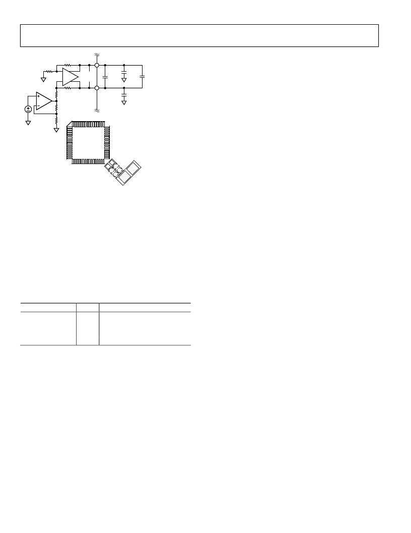
Figure 75. ADC Reference and Decoupling
The ADC has an internal voltage reference and reference ampli-
fier as shown in Figure 75. The internal band gap reference
generates a stable 1 V reference level that is converted to a
differential 1 V reference centered about mid-supply (AVDD/2).
The outputs of the differential reference amplifier are available
at the REFT and REFB pins and
must
be properly decoupled for
optimum performance. The REFT and REFB pins are conven-
iently situated at the corners of the CSP package such that C1
(0603 type) can be placed directly across its pins. C3 and C4 can
be placed underneath C1, and C2 (10 μF tantalum) can be
placed furthest from the package.
Table 21. SPI Registers for Rx ADC
Address (Hex)
Bit
Description
0x04
(5)
Duty cycle restore circuit
(4)
ADC clock from PLL
0x07
(4)
ADC low power mode
0x13
(2:0)
ADC power bias adjust
相關(guān)PDF資料 |
PDF描述 |
|---|---|
| AD9866 | Broadband Modem Mixed Signal Front End |
| AD9866-EB | Broadband Modem Mixed Signal Front End |
| AD9866BCP | Broadband Modem Mixed Signal Front End |
| AD9870 | IF Digitizing Subsystem |
| AD9870EB | IF Digitizing Subsystem |
相關(guān)代理商/技術(shù)參數(shù) |
參數(shù)描述 |
|---|---|
| AD9866-EB | 制造商:Analog Devices 功能描述: 制造商:Analog Devices 功能描述:12B MXFE CONVERTER FOR BROADBAND MODEMS - Bulk |
| AD9867 | 制造商:AD 制造商全稱:Analog Devices 功能描述:Broadband Modem Mixed-Signal Front End |
| AD9867BCPZ | 功能描述:IC MXFE 75MSPS FOR TX/RX 64LFCSP RoHS:是 類別:RF/IF 和 RFID >> RF 前端 (LNA + PA) 系列:- 產(chǎn)品培訓(xùn)模塊:Lead (SnPb) Finish for COTS Obsolescence Mitigation Program 標(biāo)準(zhǔn)包裝:250 系列:- RF 型:GPS 頻率:1575.42MHz 特點(diǎn):- 封裝/外殼:48-TQFP 裸露焊盤 供應(yīng)商設(shè)備封裝:48-TQFP 裸露焊盤(7x7) 包裝:托盤 |
| AD9867BCPZRL | 功能描述:IC MXFE 75MSPS FOR TX/RX 64LFCSP RoHS:是 類別:RF/IF 和 RFID >> RF 前端 (LNA + PA) 系列:- 產(chǎn)品培訓(xùn)模塊:Lead (SnPb) Finish for COTS Obsolescence Mitigation Program 標(biāo)準(zhǔn)包裝:250 系列:- RF 型:GPS 頻率:1575.42MHz 特點(diǎn):- 封裝/外殼:48-TQFP 裸露焊盤 供應(yīng)商設(shè)備封裝:48-TQFP 裸露焊盤(7x7) 包裝:托盤 |
| AD9867-EBZ | 制造商:Analog Devices 功能描述:12B MXFE CONVERTER FOR BROADBAND MODEMS - Bulk |
發(fā)布緊急采購(gòu),3分鐘左右您將得到回復(fù)。