- 您現在的位置:買賣IC網 > PDF目錄373975 > ADATE207BBP (ANALOG DEVICES INC) Quad Pin Timing Formatter PDF資料下載
參數資料
| 型號: | ADATE207BBP |
| 廠商: | ANALOG DEVICES INC |
| 元件分類: | 消費家電 |
| 英文描述: | Quad Pin Timing Formatter |
| 中文描述: | SPECIALTY CONSUMER CIRCUIT, PBGA256 |
| 封裝: | MO-192-BAL-2, LBGA-256 |
| 文件頁數: | 15/36頁 |
| 文件大小: | 374K |
| 代理商: | ADATE207BBP |
第1頁第2頁第3頁第4頁第5頁第6頁第7頁第8頁第9頁第10頁第11頁第12頁第13頁第14頁當前第15頁第16頁第17頁第18頁第19頁第20頁第21頁第22頁第23頁第24頁第25頁第26頁第27頁第28頁第29頁第30頁第31頁第32頁第33頁第34頁第35頁第36頁
ADATE207
Rev. 0 | Page 15 of 36
M
PER_EARLY_T0EN
PER_EARLY_C0EN
MCLK
INPUT DELAY[7:0]
CE
D
Q
T0 PIPELINE
M
M
TIMING
GENERATOR
M
0
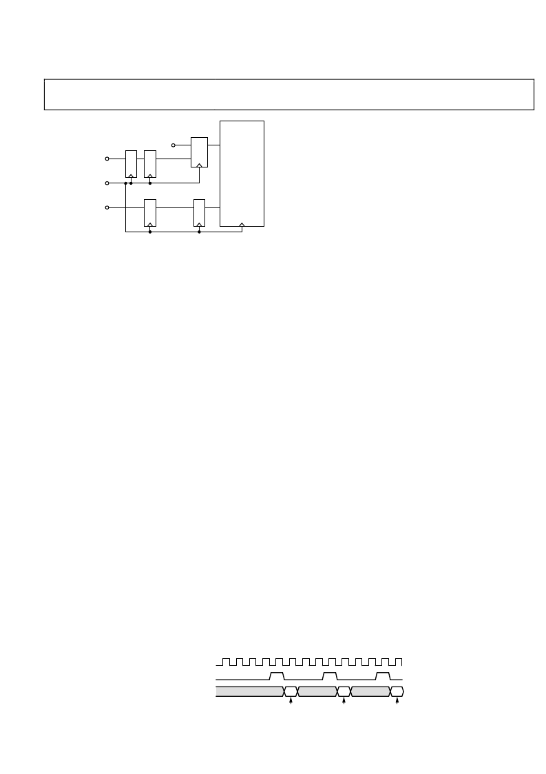
Figure 10. INPUT_DELAY Pipeline
Figure 11 shows the timing of PER_EARLY_T0EN and
the associated period delay offset, INPUT_DELAY. The
INPUT_DELAY signal is added to each programmed delay
across all channels. This input delay can change for each
PER_EARLY_T0EN period.
The delay from the pattern inputs to the DUT is four T0
pipeline delays, plus four MCLK pipeline delays, plus
approximately 27.5 ns of analog delay, plus any programmed
delay as shown in Figure 8.
The delay from the pattern inputs to the fail outputs is eight
PER_EARLY_T0EN periods plus the programmed T0
alignment pipeline depth.
DUT CAPTURE
Each compare event can strobe the state of the dual comparators
signals for each pin. These are resynchronized to T0 periods
and output for use in mixed signal capture applications. There
are four DUT capture pins per channel, PAT_DUTDATA_x and
each can be configured to output the high or low comparators
of each of the four possible compare events.
TMU MULTIPLEXER
The ADATE207 supports time measurement via an external
time measurement unit (TMU) in the following configurations:
Connect the high comparator output of any pin to
TMU_ARM, TMU_START, or TMU_STOP.
Connect the low comparator output of any pin to
TMU_ARM, TMU_START, or TMU_STOP.
The time measurement unit select logic provides time and
frequency measurement capability from the high or low
comparator outputs of any digital pin. To accomplish this
task, independent multiplexers direct the high and low
comparator outputs of the digital pins to the time measurement
unit signals, TMU_ARM, TMU_START, and TMU_STOP. Off-
chip control logic must select the appropriate TMU bus output
signal from the ADATE207 and direct its selection to the TMU.
The TMU outputs are high speed, differential 8 mA drivers and
can be tristated for bus applications.
LOW JITTER CLOCK DRIVER
The ADATE207 has 2-to-1 multiplexers in the DR_DATA_CH3
and DR_DATA_CH2 output drivers to allow an external low
jitter clock signal to drive the DCL. This feature is not available
on the DR_DATA_CH0 and DR_DATA_CH1 outputs
.
CLOCK GENERATOR MODE
The ADATE207 incorporates a clock generation mode to allow
it to be used as a programmable clock generator. In this mode, it
is possible for each of the four channels to produce an
independently programmable clock.
To activate this mode, PER_EARLY_T0EN and the
CLKGEN_MD_EN input need to be set high. In this mode,
PAT_DATA_VALID has no effect. The pattern data signals
(PAT_PATDATA_x) are interpreted as period offsets and the
PAT_MASK[x] inputs are used as period start enables. See
Table 11 for details of signal mapping. The use model for this
mode is
Program drive high/drive low operations at Address 0 in
the waveform memory. Depending on the delays, the value
per edge, the duty cycle, and the start level can be adjusted
per channel
Four different clocks can be controlled by using
PAT_MASK[N] as equivalent period start signals for an
individual Channel N.
Skew/insertion delay of the clocks can be adjusted
individually by using I_PAT_PATADATA_N as an
INPUT_DELAY signal for Channel N.
DEVICE RESET
The ADATE207 has an internal PLL and FIFO that require reset
upon power up and changes to the MCLK input. The device has
three reset controls.
RESET_B input pin for hard resets.
CPU writeable control bit (Bit 00 in Register 0x19) for soft
resets.
CPU writeable control bit (Bit 03 in Register 0x19) to reset
errors and internal FIFOs.
MCLK
PER_EARLY_T0EN
INPUT_DELAY[7:0]
DELAY
DELAY
DELAY
0
Figure 11. Timing Diagram for PER_EARLY_T0EN and INPUT_DELAY
相關PDF資料 |
PDF描述 |
|---|---|
| ADATE207BBPZ | Quad Pin Timing Formatter |
| ADAU1401 | SigmaDSP 28-/56-Bit Audio Processor with Two ADCs and Four DACs |
| ADAU1401YSTZ | SigmaDSP 28-/56-Bit Audio Processor with Two ADCs and Four DACs |
| ADAU1401YSTZ-RL | SigmaDSP 28-/56-Bit Audio Processor with Two ADCs and Four DACs |
| ADAU1513 | Class-D Audio Power Stage |
相關代理商/技術參數 |
參數描述 |
|---|---|
| ADATE207BBPZ | 功能描述:IC TIMING FORMATTER QUAD 256BGA RoHS:是 類別:集成電路 (IC) >> 時鐘/計時 - 專用 系列:- 標準包裝:1 系列:- 類型:時鐘/頻率發生器,多路復用器 PLL:是 主要目的:存儲器,RDRAM 輸入:晶體 輸出:LVCMOS 電路數:1 比率 - 輸入:輸出:1:2 差分 - 輸入:輸出:無/是 頻率 - 最大:400MHz 電源電壓:3 V ~ 3.6 V 工作溫度:0°C ~ 85°C 安裝類型:表面貼裝 封裝/外殼:16-TSSOP(0.173",4.40mm 寬) 供應商設備封裝:16-TSSOP 包裝:Digi-Reel® 其它名稱:296-6719-6 |
| ADATE209 | 制造商:AD 制造商全稱:Analog Devices 功能描述:4.0 Gbps Dual Driver |
| ADATE209BBCZ | 制造商:Analog Devices 功能描述:4.0 GBPS DUAL DRIVER - Rail/Tube |
| ADATE209BCPZ | 制造商:Analog Devices 功能描述: |
| ADATE302-02 | 制造商:AD 制造商全稱:Analog Devices 功能描述:500 MHz Dual Integrated DCL with Differential Drive/Receive, Level Setting DACs, and Per Pin PMU |
發布緊急采購,3分鐘左右您將得到回復。