- 您現在的位置:買賣IC網 > PDF目錄374033 > ADSP-21161N (Analog Devices, Inc.) DSP Microcomputer PDF資料下載
參數資料
| 型號: | ADSP-21161N |
| 廠商: | Analog Devices, Inc. |
| 元件分類: | 數字信號處理 |
| 英文描述: | DSP Microcomputer |
| 中文描述: | DSP微機 |
| 文件頁數: | 9/60頁 |
| 文件大小: | 1019K |
| 代理商: | ADSP-21161N |
第1頁第2頁第3頁第4頁第5頁第6頁第7頁第8頁當前第9頁第10頁第11頁第12頁第13頁第14頁第15頁第16頁第17頁第18頁第19頁第20頁第21頁第22頁第23頁第24頁第25頁第26頁第27頁第28頁第29頁第30頁第31頁第32頁第33頁第34頁第35頁第36頁第37頁第38頁第39頁第40頁第41頁第42頁第43頁第44頁第45頁第46頁第47頁第48頁第49頁第50頁第51頁第52頁第53頁第54頁第55頁第56頁第57頁第58頁第59頁第60頁
–9–
REV. A
ADSP-21161N
The serial ports operate at up to half the clock rate of the core,
providing each with a maximum data rate of 50 M bit/s. The serial
data pins are programmable as either a transmitter or receiver,
providing greater flexibility for serial communications. Serial port
data can be automatically transferred to and from on-chip
memory via a dedicated DMA. Each of the serial ports features
a Time Division Multiplex (TDM) multichannel mode, where
two serial ports are TDM transmitters and two serial ports are
TDM receivers (SPORT0 Rx paired with SPORT2 Tx,
SPORT1 Rx paired with SPORT3 Tx). Each of the serial ports
also support the I
2
S protocol (an industry standard interface
commonly used by audio codecs, ADCs and DACs), with two
data pins, allowing four I
2
S channels (using two I
2
S stereo
devices) per serial port, with a maximum of up to 16 I
2
S channels.
The serial ports permit little-endian or big-endian transmission
formats and word lengths selectable from 3 bits to 32 bits. For
I
2
S mode, data-word lengths are selectable between 8 bits and 32
bits. Serial ports offer selectable synchronization and transmit
modes as well as optional μ-law or A-law companding. Serial port
clocks and frame syncs can be internally or externally generated.
Serial Peripheral (Compatible) Interface
Serial Peripheral Interface (SPI) is an industry standard synchro-
nous serial link, enabling the ADSP-21161N SPI-compatible
port to communicate with other SPI-compatible devices. SPI is
a 4-wire interface consisting of two data pins, one device select
pin, and one clock pin. It is a full-duplex synchronous serial
interface, supporting both master and slave modes. The SPI port
can operate in a multimaster environment by interfacing with up
to four other SPI-compatible devices, either acting as a master or
slave device. The ADSP-21161N SPI-compatible peripheral
implementation also features programmable baud rate and clock
phase/polarities. The ADSP-21161N SPI-compatible port uses
open drain drivers to support a multimaster configuration and to
avoid data contention.
Host Processor Interface
The ADSP-21161N host interface enables easy connection to
standard 8-bit, 16-bit, or 32-bit microprocessor buses with little
additional hardware required. The host interface is accessed
through the ADSP-21161N’s external port. Four channels of
DMA are available for the host interface; code and data transfers
are accomplished with low software overhead. The host processor
requests the ADSP-21161N’s external bus with the host bus
request (
HBR
), host bus grant (
HBG
), and chip select (CS)
signals. The host can directly read and write the internal IOP
registers of the ADSP-21161N, and can access the DMA channel
setup and message registers. DMA setup via a host would allow
it to access any internal memory address via DMA transfers.
Vector interrupt support provides efficient execution of host
commands.
General-Purpose I/O Ports
The ADSP-21161N also contains 12 programmable, general
purpose I/O pins that can function as either input or output. As
output, these pins can signal peripheral devices; as input, these
pins can provide the test for conditional branching.
Program Booting
The internal memory of the ADSP-21161N can be booted at
system power-up from either an 8-bit EPROM, a host processor,
the SPI interface, or through one of the link ports. Selection of
the boot source is controlled by the Boot Memory Select (
BMS
),
EBOOT (EPROM Boot), and Link/Host Boot (LBOOT) pins.
8-, 16-, or 32-bit host processors can also be used for booting.
Phase-Locked Loop and Crystal Double Enable
The ADSP-21161N uses an on-chip Phase-Locked Loop (PLL)
to generate the internal clock for the core. The CLK_CFG1
–
0
pins are used to select ratios of 2:1, 3:1, and 4:1. In addition to
the PLL ratios, the
CLKDBL
pin can be used for more clock
ratio options. The (1
×
/2
×
CLKIN) rate set by the
CLKDBL
pin determines the rate of the PLL input clock and the rate at
which the external port operates. With the combination of
CLK_CFG1
–
0 and
CLKDBL
, ratios of 2:1, 3:1, 4:1, 6:1, and
8:1 between the core and CLKIN are supported. See also
Figure 10 on Page 20
.
Power Supplies
The ADSP-21161N has separate power supply connections for
the analog (AV
DD
/AGND), internal (V
DDINT
), and external
(V
DDEXT
) power supplies. The internal and analog supplies must
meet the 1.8 V requirement. The external supply must meet the
3.3 V requirement. All external supply pins must be connected
to the same supply.
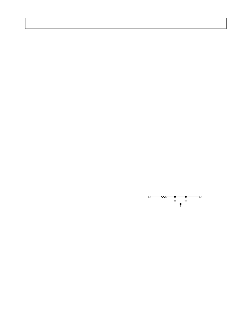
Note that the analog supply (AV
DD
) powers the ADSP-21161N’s
clock generator PLL. To produce a stable clock, provide an
external circuit to filter the power input to the AV
DD
pin. Place
the filter as close as possible to the pin. For an example circuit,
see
Figure 5
. To prevent noise coupling, use a wide trace for the
analog ground (AGND) signal and install a decoupling capacitor
as close as possible to the pin.
Development Tools
The ADSP-21161N is supported with a complete set of software
and hardware development tools, including Analog Devices
emulators and VisualDSP++
1
development environment. The
same emulator hardware that supports other ADSP-21xxx DSPs,
also fully emulates the ADSP-21161N.
The VisualDSP++ project management environment lets pro-
grammers develop and debug an application. This environment
includes an easy-to-use assembler that is based on an algebraic
syntax; an archiver (librarian/library builder), a linker, a loader,
Figure 5. Analog Power (AV
DD
) Filter Circuit
1
VisualDSP++ is a registered trademark of Analog Devices, Inc.
10
V
DDINT
0.1 F
0.01 F
AGND
AV
DD
相關PDF資料 |
PDF描述 |
|---|---|
| ADSP-21161NCCA-100 | DSP Microcomputer |
| ADSP-21161NKCA-100 | DSP Microcomputer |
| ADSP-21262SBBC-150 | Embedded Processor |
| ADSP-21262SBBCZ150 | Embedded Processor |
| ADSP-21262SKSTZ200 | SHARC Processor |
相關代理商/技術參數 |
參數描述 |
|---|---|
| ADSP-21161NCCA-100 | 功能描述:IC DSP CONTROLLER 32BIT 225MBGA RoHS:否 類別:集成電路 (IC) >> 嵌入式 - DSP(數字式信號處理器) 系列:SHARC® 標準包裝:2 系列:StarCore 類型:SC140 內核 接口:DSI,以太網,RS-232 時鐘速率:400MHz 非易失內存:外部 芯片上RAM:1.436MB 電壓 - 輸入/輸出:3.30V 電壓 - 核心:1.20V 工作溫度:-40°C ~ 105°C 安裝類型:表面貼裝 封裝/外殼:431-BFBGA,FCBGA 供應商設備封裝:431-FCPBGA(20x20) 包裝:托盤 |
| ADSP-21161NCCAZ100 | 功能描述:IC DSP CONTROLLER 32BIT 225MBGA RoHS:是 類別:集成電路 (IC) >> 嵌入式 - DSP(數字式信號處理器) 系列:SHARC® 標準包裝:2 系列:StarCore 類型:SC140 內核 接口:DSI,以太網,RS-232 時鐘速率:400MHz 非易失內存:外部 芯片上RAM:1.436MB 電壓 - 輸入/輸出:3.30V 電壓 - 核心:1.20V 工作溫度:-40°C ~ 105°C 安裝類型:表面貼裝 封裝/外殼:431-BFBGA,FCBGA 供應商設備封裝:431-FCPBGA(20x20) 包裝:托盤 |
| ADSP-21161NKCA-100 | 功能描述:IC DSP CONTROLLER 32BIT 225MBGA RoHS:否 類別:集成電路 (IC) >> 嵌入式 - DSP(數字式信號處理器) 系列:SHARC® 標準包裝:2 系列:StarCore 類型:SC140 內核 接口:DSI,以太網,RS-232 時鐘速率:400MHz 非易失內存:外部 芯片上RAM:1.436MB 電壓 - 輸入/輸出:3.30V 電壓 - 核心:1.20V 工作溫度:-40°C ~ 105°C 安裝類型:表面貼裝 封裝/外殼:431-BFBGA,FCBGA 供應商設備封裝:431-FCPBGA(20x20) 包裝:托盤 |
| ADSP-21161NKCA-100Z | 制造商:Analog Devices 功能描述: |
| ADSP-21161NKCAZ100 | 功能描述:IC DSP CONTROLLER 32BIT 225MBGA RoHS:是 類別:集成電路 (IC) >> 嵌入式 - DSP(數字式信號處理器) 系列:SHARC® 標準包裝:2 系列:StarCore 類型:SC140 內核 接口:DSI,以太網,RS-232 時鐘速率:400MHz 非易失內存:外部 芯片上RAM:1.436MB 電壓 - 輸入/輸出:3.30V 電壓 - 核心:1.20V 工作溫度:-40°C ~ 105°C 安裝類型:表面貼裝 封裝/外殼:431-BFBGA,FCBGA 供應商設備封裝:431-FCPBGA(20x20) 包裝:托盤 |
發布緊急采購,3分鐘左右您將得到回復。