- 您現在的位置:買賣IC網 > PDF目錄374037 > ADSP-21MOD980N (Analog Devices, Inc.) MultiPort Internet Gateway Processor PDF資料下載
參數資料
| 型號: | ADSP-21MOD980N |
| 廠商: | Analog Devices, Inc. |
| 英文描述: | MultiPort Internet Gateway Processor |
| 中文描述: | 通寶互聯網網關處理器 |
| 文件頁數: | 23/42頁 |
| 文件大小: | 566K |
| 代理商: | ADSP-21MOD980N |
第1頁第2頁第3頁第4頁第5頁第6頁第7頁第8頁第9頁第10頁第11頁第12頁第13頁第14頁第15頁第16頁第17頁第18頁第19頁第20頁第21頁第22頁當前第23頁第24頁第25頁第26頁第27頁第28頁第29頁第30頁第31頁第32頁第33頁第34頁第35頁第36頁第37頁第38頁第39頁第40頁第41頁第42頁
23
REV. PrB
6/2001
For current information contact Analog Devices at (800) ANALOGD
ADSP-21mod980N
PRELIMINARY TECHNICAL DATA
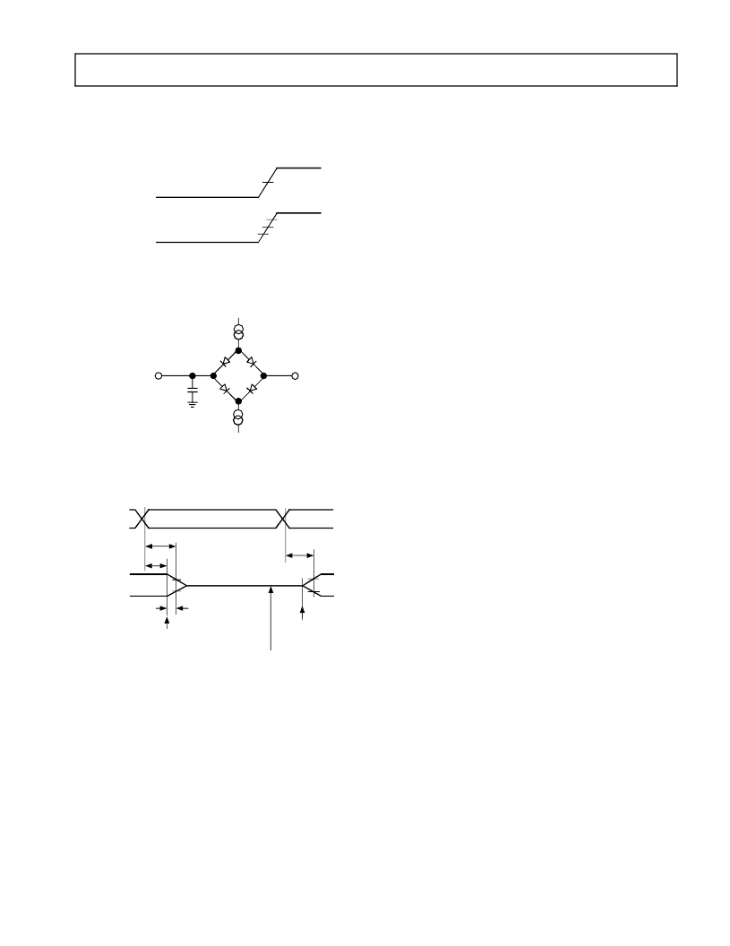
TEST CONDITIONS
Output Disable Time
Output pins are considered to be disabled when they have
stopped driving and started a transition from the measured
output high or low voltage to a high impedance state. The
output disable time (t
DIS
) is the difference of t
MEASURED
and
t
DECAY
, as shown in
Figure 16
. The time is the interval from
when a reference signal reaches a high or low voltage level
to when the output voltages have changed by 0.5 V from the
measured output high or low voltage.
The decay time, t
DECAY
, is dependent on the capacitive load,
C
L
, and the current load, i
L
, on the output pin. It can be
approximated by the following equation:
from which
is calculated. If multiple pins (such as the data bus) are dis-
abled, the measurement value is that of the last pin to stop
driving.
Output Enable Time
Output pins are considered to be enabled when they have
made a transition from a high-impedance state to when they
start driving. The output enable time (t
ENA
) is the interval
from when a reference signal reaches a high or low voltage
level to when the output has reached a specified high or low
trip point, as shown in
Figure 16
. If multiple pins (such as
the data bus) are enabled, the measurement value is that of
the first pin to start driving.
Figure 14. Voltage Reference Levels for AC
Measurements (Except Output Enable/Disable)
Figure 15. Equivalent Loading for AC Measurements
(Including All Fixtures)
Figure 16. Output Enable/Disable
1.5V
OUTPUT
INPUT
1.5V
0.8V
2.0V
TO
OUTPUT
PIN
50pF
1.5V
I
OH
I
OL
2.0V
1.0V
t
ENA
REFERENCE
SIGNAL
OUTPUT
t
DECAY
V
OH
(MEASURED)
OUTPUT STOPS
DRIVING
OUTPUT STARTS
DRIVING
t
DIS
t
MEASURED
V
OL
(MEASURED)
V
OH
(MEASURED) - 0.5V
V
OL
(MEASURED) +0.5V
HIGH-IMPEDANCE STATE. TEST CONDITIONS CAUSE
THIS VOLTAGE LEVEL TO BE APPROXIMATELY 1.5V.
V
OH
(MEASURED)
V
OL
(MEASURED)
t
DECAY
C
-------------------------
0.5
V
i
L
=
t
DIS
t
MEASURED
t
DECAY
–
=
相關PDF資料 |
PDF描述 |
|---|---|
| ADSP-21MOD980N-000 | CAP 27PF 100V 10% X7R AXIAL BULK M-MIL-PRF-39014 |
| ADSP-21MSP58BST-104 | DSP Microcomputers |
| ADSP-BF531 | Blackfin Embedded Processor |
| ADSP-BF531SBBC400 | Metal Connector Backshell |
| ADSP-BF531SBBZ400 | Blackfin Embedded Processor |
相關代理商/技術參數 |
參數描述 |
|---|---|
| ADSP-21MSP50ABG-52 | 制造商:Analog Devices 功能描述: |
| adsp-21msp50akg-52 | 制造商:Rochester Electronics LLC 功能描述:- Bulk 制造商:Analog Devices 功能描述: |
| ADSP-21MSP50BG-52 | 制造商:Rochester Electronics LLC 功能描述:- Bulk |
| ADSP-21MSP50KG-52 | 制造商:Rochester Electronics LLC 功能描述:- Bulk |
| ADSP-21MSP52-520010 | 制造商:Analog Devices 功能描述: |
發布緊急采購,3分鐘左右您將得到回復。