- 您現在的位置:買賣IC網 > PDF目錄21992 > EP2AGX125EF29C5N (Altera)IC ARRIA II GX FPGA 125K 780FBGA PDF資料下載
參數資料
| 型號: | EP2AGX125EF29C5N |
| 廠商: | Altera |
| 文件頁數: | 70/90頁 |
| 文件大小: | 0K |
| 描述: | IC ARRIA II GX FPGA 125K 780FBGA |
| 產品培訓模塊: | Arria II GX FPGA Three Reasons to Use FPGA's in Industrial Designs |
| 標準包裝: | 4 |
| 系列: | Arria II GX |
| LAB/CLB數: | 4964 |
| 邏輯元件/單元數: | 118143 |
| RAM 位總計: | 8315904 |
| 輸入/輸出數: | 372 |
| 電源電壓: | 0.87 V ~ 0.93 V |
| 安裝類型: | 表面貼裝 |
| 工作溫度: | 0°C ~ 85°C |
| 封裝/外殼: | 780-BBGA |
| 供應商設備封裝: | 780-FBGA(29x29) |
| 其它名稱: | 544-2645 |
第1頁第2頁第3頁第4頁第5頁第6頁第7頁第8頁第9頁第10頁第11頁第12頁第13頁第14頁第15頁第16頁第17頁第18頁第19頁第20頁第21頁第22頁第23頁第24頁第25頁第26頁第27頁第28頁第29頁第30頁第31頁第32頁第33頁第34頁第35頁第36頁第37頁第38頁第39頁第40頁第41頁第42頁第43頁第44頁第45頁第46頁第47頁第48頁第49頁第50頁第51頁第52頁第53頁第54頁第55頁第56頁第57頁第58頁第59頁第60頁第61頁第62頁第63頁第64頁第65頁第66頁第67頁第68頁第69頁當前第70頁第71頁第72頁第73頁第74頁第75頁第76頁第77頁第78頁第79頁第80頁第81頁第82頁第83頁第84頁第85頁第86頁第87頁第88頁第89頁第90頁
1–64
Chapter 1: Device Datasheet for Arria II Devices
Switching Characteristics
December 2013
Altera Corporation
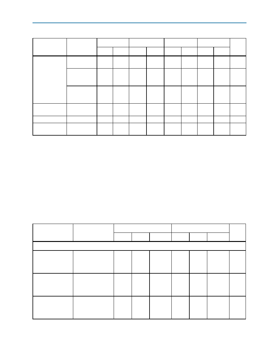
Table 1–54 lists the high-speed I/O timing for Arria II GZ devices.
fHSDR (data rate)
SERDES factor
J = 3 to 10
945
945
740
640
Mbps
SERDES factor
J = 2 (using
DDR registers)
Mbps
SERDES factor
J = 1 (using
SDR registers)
Mbps
Soft-CDR PPM
tolerance
Soft-CDR
mode
—
300
—
300
—
300
—
300
PPM
DPA run length
DPA mode
—
10,000
—
10,000
—
10,000
—
10,000
UI
Sampling
window (SW)
Non-DPA mode
—
300
—
300
—
350
—
400
ps
Notes to Table 1–53:
(1) fHSCLK_IN = fHSDR / W. Use W to determine the supported selection of input reference clock frequencies for the desired data rate.
(2) Applicable for interfacing with DPA receivers only. For interfacing with non-DPA receivers, you must calculate the leftover timing margin in the
receiver by performing link timing closure analysis. For Arria II GX transmitter to Arria II GX non-DPA receiver, the maximum supported data
rate is 945 Mbps. For data rates above 840 Mbps, perform PCB trace compensation by adjusting the PCB trace length for LVDS channels to
improve channel-to-channel skews.
(3) The minimum and maximum specification depends on the clock source (for example, PLL and clock pin) and the clock routing resource you
use (global, regional, or local). The I/O differential buffer and input register do not have a minimum toggle rate.
(4) The specification is only applicable under the influence of core noise.
(5) Applicable for true LVDS using dedicated SERDES only.
(6) Dedicated SERDES and DPA features are only available on the right banks.
(7) You must calculate the leftover timing margin in the receiver by performing link timing closure analysis. You must consider the board skew
margin, transmitter channel-to-channel skew, and the receiver sampling margin to determine the leftover timing margin.
Table 1–53. High-Speed I/O Specifications for Arria II GX Devices (Part 4 of 4)
Symbol
Conditions
I3
C4
C5,I5
C6
Unit
Min
Max
Min
Max
Min
Max
Min
Max
Table 1–54. High-Speed I/O Specifications for Arria II GZ Devices (Note 1), (2), (10) (Part 1 of 3)
Symbol
Conditions
C3, I3
C4, I4
Unit
Min
Typ
Max
Min
Typ
Max
Clock
fHSCLK_in (input clock
frequency) true
differential I/O
standards
Clock boost factor
W = 1 to 40 (3)
5
—
717
5
—
717
MHz
fHSCLK_in (input clock
frequency) single
ended I/O standards
Clock boost factor
W = 1 to 40 (3)
5
—
717
5
—
717
MHz
fHSCLK_in (input clock
frequency) single
ended I/O standards
Clock boost factor
W = 1 to 40 (3)
5
—
420
5
—
420
MHz
相關PDF資料 |
PDF描述 |
|---|---|
| DS1722X/T&R | IC THERMOMETER DIG 3-WIRE 8FCHIP |
| AIMC-0805-2N7S-T | INDUCTOR MULTILAYER 2.7NH 0805 |
| VJ1206A681KBEAT4X | CAP CER 680PF 500V 10% NP0 1206 |
| HBM08DRYI-S13 | CONN EDGECARD 16POS .156 EXTEND |
| VI-274-CW-F2 | CONVERTER MOD DC/DC 48V 100W |
相關代理商/技術參數 |
參數描述 |
|---|---|
| EP2AGX125EF29C5NES | 制造商:Altera Corporation 功能描述:FPGA Arria |
| EP2AGX125EF29C6 | 功能描述:FPGA - 現場可編程門陣列 FPGA - Arria II GX 4964 LABs 372 IOs RoHS:否 制造商:Altera Corporation 系列:Cyclone V E 柵極數量: 邏輯塊數量:943 內嵌式塊RAM - EBR:1956 kbit 輸入/輸出端數量:128 最大工作頻率:800 MHz 工作電源電壓:1.1 V 最大工作溫度:+ 70 C 安裝風格:SMD/SMT 封裝 / 箱體:FBGA-256 |
| EP2AGX125EF29C6ES | 制造商:Altera Corporation 功能描述:FPGA Arria |
| EP2AGX125EF29C6N | 功能描述:FPGA - 現場可編程門陣列 FPGA - Arria II GX 4964 LABs 372 IOs RoHS:否 制造商:Altera Corporation 系列:Cyclone V E 柵極數量: 邏輯塊數量:943 內嵌式塊RAM - EBR:1956 kbit 輸入/輸出端數量:128 最大工作頻率:800 MHz 工作電源電壓:1.1 V 最大工作溫度:+ 70 C 安裝風格:SMD/SMT 封裝 / 箱體:FBGA-256 |
| EP2AGX125EF29C6NES | 制造商:Altera Corporation 功能描述:FPGA Arria |
發布緊急采購,3分鐘左右您將得到回復。