- 您現(xiàn)在的位置:買賣IC網(wǎng) > PDF目錄21992 > EP2AGX125EF29C5N (Altera)IC ARRIA II GX FPGA 125K 780FBGA PDF資料下載
參數(shù)資料
| 型號: | EP2AGX125EF29C5N |
| 廠商: | Altera |
| 文件頁數(shù): | 76/90頁 |
| 文件大小: | 0K |
| 描述: | IC ARRIA II GX FPGA 125K 780FBGA |
| 產(chǎn)品培訓(xùn)模塊: | Arria II GX FPGA Three Reasons to Use FPGA's in Industrial Designs |
| 標(biāo)準(zhǔn)包裝: | 4 |
| 系列: | Arria II GX |
| LAB/CLB數(shù): | 4964 |
| 邏輯元件/單元數(shù): | 118143 |
| RAM 位總計: | 8315904 |
| 輸入/輸出數(shù): | 372 |
| 電源電壓: | 0.87 V ~ 0.93 V |
| 安裝類型: | 表面貼裝 |
| 工作溫度: | 0°C ~ 85°C |
| 封裝/外殼: | 780-BBGA |
| 供應(yīng)商設(shè)備封裝: | 780-FBGA(29x29) |
| 其它名稱: | 544-2645 |
第1頁第2頁第3頁第4頁第5頁第6頁第7頁第8頁第9頁第10頁第11頁第12頁第13頁第14頁第15頁第16頁第17頁第18頁第19頁第20頁第21頁第22頁第23頁第24頁第25頁第26頁第27頁第28頁第29頁第30頁第31頁第32頁第33頁第34頁第35頁第36頁第37頁第38頁第39頁第40頁第41頁第42頁第43頁第44頁第45頁第46頁第47頁第48頁第49頁第50頁第51頁第52頁第53頁第54頁第55頁第56頁第57頁第58頁第59頁第60頁第61頁第62頁第63頁第64頁第65頁第66頁第67頁第68頁第69頁第70頁第71頁第72頁第73頁第74頁第75頁當(dāng)前第76頁第77頁第78頁第79頁第80頁第81頁第82頁第83頁第84頁第85頁第86頁第87頁第88頁第89頁第90頁
1–70
Chapter 1: Device Datasheet for Arria II Devices
Switching Characteristics
December 2013
Altera Corporation
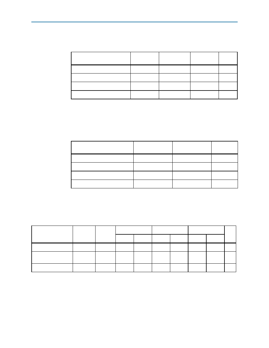
Table 1–60 lists the DQS phase shift error for Arria II GX devices.
Table 1–61 lists the DQS phase shift error for Arria II GZ devices.
Table 1–62 lists the memory output clock jitter specifications for Arria II GX devices.
Table 1–60. DQS Phase Shift Error Specification for DLL-Delayed Clock (tDQS_PSERR) for Arria II GX
Devices (Note 1)
Number of DQS Delay Buffer
C4
I3, C5, I5
C6
Unit
1
263036
ps
2
526072
ps
3
78
90
108
ps
4
104
120
144
ps
Note to Table 1–60:
(1) This error specification is the absolute maximum and minimum error. For example, skew on three DQS delay
buffers in a C4 speed grade is ± 78 ps or ± 39 ps.
Table 1–61. DQS Phase Shift Error Specification for DLL-Delayed Clock (tDQS_PSERR) for Arria II GZ
Devices (Note 1)
Number of DQS Delay Buffer
–3
–4
Unit
128
30
ps
256
60
ps
384
90
ps
4
112
120
ps
Note to Table 1–61:
(1) This error specification is the absolute maximum and minimum error. For example, skew on three DQS delay
buffers in a 3 speed grade is ± 84 ps or ± 42 ps.
Parameter
Clock
Network
Symbol
–4
–5
–6
Unit
Min
Max
Min
Max
Min
Max
Clock period jitter
Global
t
JIT(per)
-100
100
-125
125
-125
125
ps
Cycle-to-cycle period
jitter
Global
t
JIT(cc)
-200
200
-250
250
-250
250
ps
Duty cycle jitter
Global
t
JIT(duty)
-100
100
-125
125
-125
125
ps
Notes to Table 1–62:
(1) The memory output clock jitter measurements are for 200 consecutive clock cycles, as specified in the JEDEC DDR2/DDR3 SDRAM standard.
(2) The clock jitter specification applies to memory output clock pins generated using DDIO circuits clocked by a PLL output routed on a global
clock network.
(3) The memory output clock jitter stated in Table 1–62 is applicable when an input jitter of 30 ps is applied.
相關(guān)PDF資料 |
PDF描述 |
|---|---|
| DS1722X/T&R | IC THERMOMETER DIG 3-WIRE 8FCHIP |
| AIMC-0805-2N7S-T | INDUCTOR MULTILAYER 2.7NH 0805 |
| VJ1206A681KBEAT4X | CAP CER 680PF 500V 10% NP0 1206 |
| HBM08DRYI-S13 | CONN EDGECARD 16POS .156 EXTEND |
| VI-274-CW-F2 | CONVERTER MOD DC/DC 48V 100W |
相關(guān)代理商/技術(shù)參數(shù) |
參數(shù)描述 |
|---|---|
| EP2AGX125EF29C5NES | 制造商:Altera Corporation 功能描述:FPGA Arria |
| EP2AGX125EF29C6 | 功能描述:FPGA - 現(xiàn)場可編程門陣列 FPGA - Arria II GX 4964 LABs 372 IOs RoHS:否 制造商:Altera Corporation 系列:Cyclone V E 柵極數(shù)量: 邏輯塊數(shù)量:943 內(nèi)嵌式塊RAM - EBR:1956 kbit 輸入/輸出端數(shù)量:128 最大工作頻率:800 MHz 工作電源電壓:1.1 V 最大工作溫度:+ 70 C 安裝風(fēng)格:SMD/SMT 封裝 / 箱體:FBGA-256 |
| EP2AGX125EF29C6ES | 制造商:Altera Corporation 功能描述:FPGA Arria |
| EP2AGX125EF29C6N | 功能描述:FPGA - 現(xiàn)場可編程門陣列 FPGA - Arria II GX 4964 LABs 372 IOs RoHS:否 制造商:Altera Corporation 系列:Cyclone V E 柵極數(shù)量: 邏輯塊數(shù)量:943 內(nèi)嵌式塊RAM - EBR:1956 kbit 輸入/輸出端數(shù)量:128 最大工作頻率:800 MHz 工作電源電壓:1.1 V 最大工作溫度:+ 70 C 安裝風(fēng)格:SMD/SMT 封裝 / 箱體:FBGA-256 |
| EP2AGX125EF29C6NES | 制造商:Altera Corporation 功能描述:FPGA Arria |
發(fā)布緊急采購,3分鐘左右您將得到回復(fù)。