- 您現在的位置:買賣IC網 > PDF目錄98215 > TFP420PAP (TEXAS INSTRUMENTS INC) SPECIALTY CONSUMER CIRCUIT, PQFP64 PDF資料下載
參數資料
| 型號: | TFP420PAP |
| 廠商: | TEXAS INSTRUMENTS INC |
| 元件分類: | 消費家電 |
| 英文描述: | SPECIALTY CONSUMER CIRCUIT, PQFP64 |
| 封裝: | 10 X 10 MM, 1.40 MM HEIGHT, 0.50 MM PITCH, POWER, THERMALLY ENHANCED, PLASTIC, TQFP-64 |
| 文件頁數: | 15/20頁 |
| 文件大?。?/td> | 253K |
| 代理商: | TFP420PAP |
TFP420
PanelBus
DIGITAL TRANSMITTER
SLDS123A – MARCH 2000 – REVISED JUNE 2000
4
POST OFFICE BOX 655303
DALLAS, TEXAS 75265
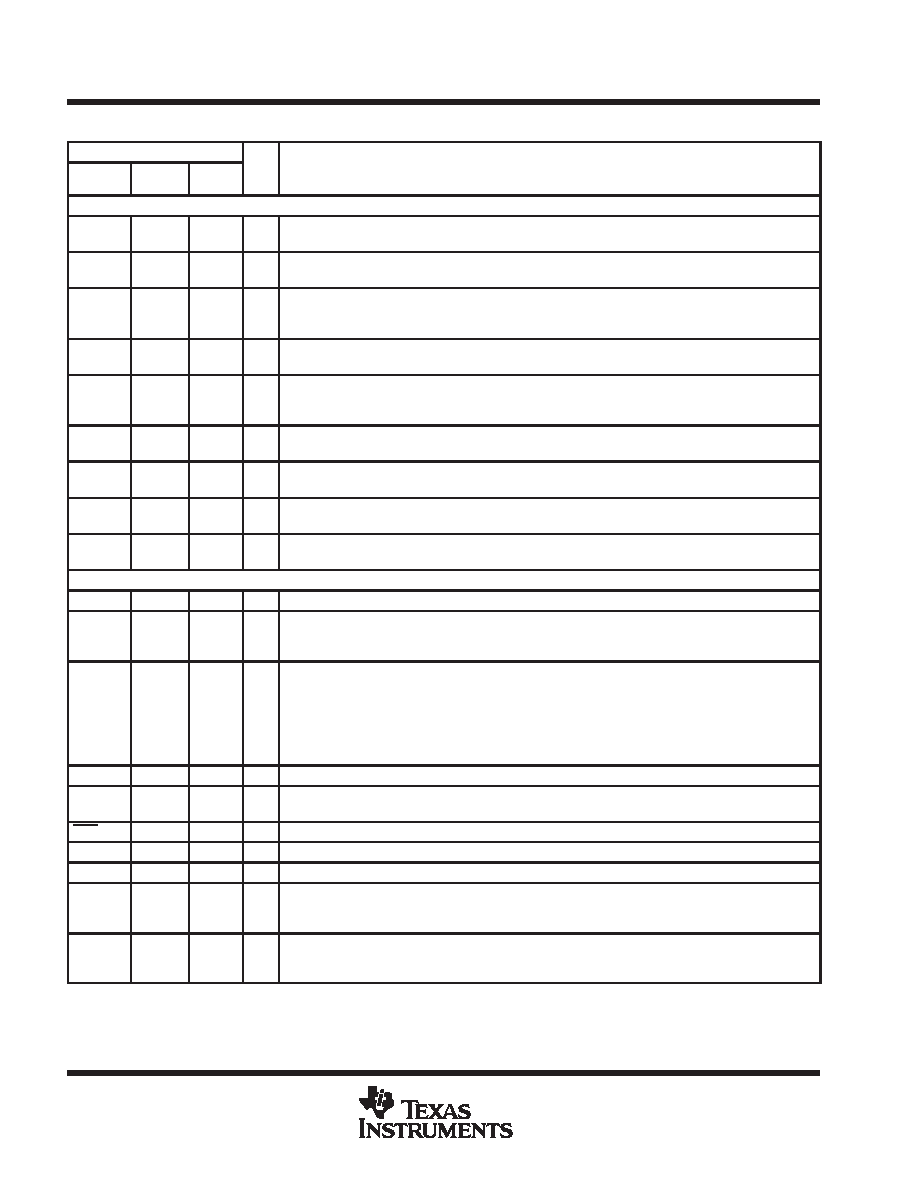
Terminal Functions (Continued)
TERMINAL
NAME
POWER
RAIL
NO.
I/O
DESCRIPTION
DVI Output
TX2+
TVDD
28
A
Red channel positive transmitter output – Positive side of red channel T.M.D.S. low voltage signal
differential output pair. Red channel transmits red pixel data in active display and 00 control bits in blank.
TX2–
TVDD
27
A
Red channel negative transmitter output – Negative side of red channel T.M.D.S. low voltage signal
differential output pair.
TX1+
TVDD
25
A
Green channel positive transmitter output – Positive side of green channel T.M.D.S. low voltage signal
differential output pair. Green channel transmits green pixel data in active display and 00 control bits in
blank.
TX1–
TVDD
24
A
Green channel negative transmitter output – Negative side of green channel T.M.D.S. low voltage signal
differential output pair.
TX0+
TVDD
22
A
Blue channel positive transmitter output – Positive side of blue channel T.M.D.S. low voltage signal
differential output pair. Blue channel transmits blue pixel data in active display and HSYNC, VSYNC
control signals in blank.
TX0–
TVDD
21
A
Blue channel negative transmitter output – Negative side of blue channel T.M.D.S. low voltage signal
differential output pair.
TXC+
TVDD
30
A
Clock positive transmitter output – Positive side of reference clock T.M.D.S. low voltage signal
differential output pair.
TXC–
TVDD
31
A
Clock negative transmitter output – Negative side of reference clock T.M.D.S. low voltage signal
differential output pair.
TFADJ
TVDD
19
A
T.M.D.S. drivers full scale adjust control
A 2-k
resistor must be connected between this terminal and TVSS.
I2C Interface and Miscellaneous
A0
DVCC
10
I
I2C slave address select
GPIO0
DVCC
18
I/O
General-purpose I/O #0
First general-purpose I/O. This terminal has an internal weak pulldown of 1 M
(TBD). With GPIO0 as
an input, use an external 10 k
resistor to pull up or down to set the state of this terminal.
HS/CS/
GPIO1
AVCC
45
I/O
Digital horizontal sync output – This is the HSYNC signal that connects to the VGA connector.
Digital composite sync output – Composite HSYNC and VSYNC. The polarity of this signal is
programmable when used for HS/CS.
General-purpose I/O #1 – Second general-purpose I/O. This terminal has an internal weak pulldown of
1 M
(TBD). With GPIO1 as an input, use an external 10-k resistor to pull up or down to set the state of
this terminal.
HTPLG
DVCC
11
I
DVI/P&D/DFP hot plug detect input
NC
AVCC
38–41,
43, 44
A
Reserved
RST
DVCC
13
I
Reset signal active low.
SCL
DVCC
15
I/O
I2C serial clock input maximum. Clock rate of 400 kHz. Open drained I/O.
SDA
DVCC
14
I/O
I2C Serial data line open drained I/O.
TEST
DVCC
17
I
Test mode enable
This terminal must be tied to LOW for normal mode of operation. Connecting this terminal to HIGH puts
TFP420 in test mode.
VS
AVCC
46
O
Digital vertical sync output
When the analog RGB video output is enabled this signal is the VSYNC that connects to the VGA
connector.
相關PDF資料 |
PDF描述 |
|---|---|
| TFP501PZPG4 | SPECIALTY CONSUMER CIRCUIT, PQFP100 |
| TFP501PZP | SPECIALTY CONSUMER CIRCUIT, PQFP100 |
| TFP503PZPG4 | SPECIALTY CONSUMER CIRCUIT, PQFP100 |
| TFP503PZP | SPECIALTY CONSUMER CIRCUIT, PQFP100 |
| TFP510PAPG4 | SPECIALTY CONSUMER CIRCUIT, PQFP64 |
相關代理商/技術參數 |
參數描述 |
|---|---|
| TFP424 | 制造商:Pentair Technical Products / Hoffman 功能描述:4 in Fan Package 24 VDC , 24vdc, |
| TFP42SS | 制造商:Pentair Technical Products / Hoffman 功能描述:230V,50/60Hz,16/14W,0.14/0.11A , 230v 50/60Hz, SS Type 304 |
| TFP42UL12 | 制造商:Pentair Technical Products / Hoffman 功能描述:230V,50/60Hz,16/14W,0.14/0.11A , 230v 50/60Hz, |
| TFP4N60 | 制造商:TAK_CHEONG 制造商全稱:Tak Cheong Electronics (Holdings) Co.,Ltd 功能描述:N-Channel Power MOSFET 4.1A, 600V, 2.5Ω |
| TFP4N65 | 制造商:TAK_CHEONG 制造商全稱:Tak Cheong Electronics (Holdings) Co.,Ltd 功能描述:N-Channel Power MOSFET 3.9A, 650V, 3.0Ω |
發布緊急采購,3分鐘左右您將得到回復。