- 您現在的位置:買賣IC網 > PDF目錄98215 > TFP420PAP (TEXAS INSTRUMENTS INC) SPECIALTY CONSUMER CIRCUIT, PQFP64 PDF資料下載
參數資料
| 型號: | TFP420PAP |
| 廠商: | TEXAS INSTRUMENTS INC |
| 元件分類: | 消費家電 |
| 英文描述: | SPECIALTY CONSUMER CIRCUIT, PQFP64 |
| 封裝: | 10 X 10 MM, 1.40 MM HEIGHT, 0.50 MM PITCH, POWER, THERMALLY ENHANCED, PLASTIC, TQFP-64 |
| 文件頁數: | 18/20頁 |
| 文件大小: | 253K |
| 代理商: | TFP420PAP |
TFP420
PanelBus
DIGITAL TRANSMITTER
SLDS123A – MARCH 2000 – REVISED JUNE 2000
7
POST OFFICE BOX 655303
DALLAS, TEXAS 75265
I2C interface (continued)
Following a start condition, each I2C device decodes the slave address. The TFP420 responds with an
acknowledge by pulling the SDA line low during the ninth clock cycle if it decodes the address as its address.
During subsequent subaddress and data cycles the TFP420 responds with acknowledge as shown in Figure 3.
The subaddress is autoincremented after each data cycle.
The transmitting device must not drive the SDA signal during the acknowledge cycle so that the receiving device
may drive the SDA signal low. The not acknowledge, /A, condition is indicated by the master by keeping the SDA
signal high just before it asserts the stop, P, condition. This sequence terminates a read cycle as shown in
Figure 4.
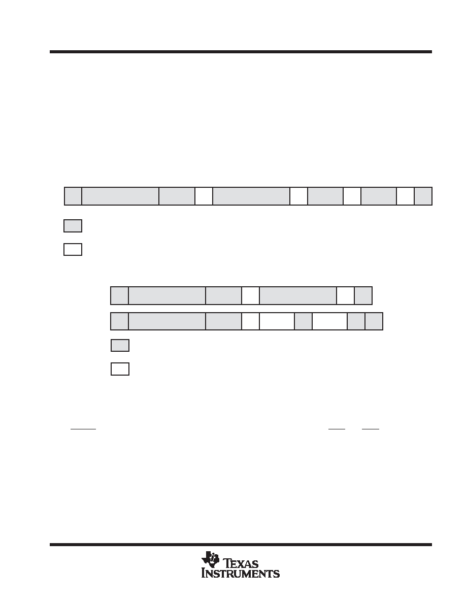
The slave address consists of 7 bits of address along with 1 bit of read/write information as shown below in
Figures 3 and 4. For the TFP420, the possible slave addresses (including the r/w bit) are 0x40 and 0x42 for write
cycles and 0x41 and 0x43 for read cycles. Refer to register description, for additional base address information.
S
Slave Address
W
Subaddress
A
Data
A
Data
A
P
From Transmitter
From Receiver
/
Not Acknowledge (SDA A High)
A
Acknowledge
S
Start Condition
P
Stop Condition
Figure 3. I2C Write Cycle
S
Slave Address
R
Data
A
S
Slave Address
W
Subaddress
A
P
Data
/A
P
From Transmitter
From Receiver
/
Not Acknowledge (SDA A High)
A
Acknowledge
S
Start Condition
P
Stop Condition
Figure 4. I2C Read Cycle
video port
The TFP420 video port is a low terminal count and high-speed digital interface. The video port consists of a
12-bit data bus (DATA[11:0]), horizontal timing signal (HSYNC), vertical timing signal (VSYNC), blanking control
(BLANK), clock signals (CLKIN0 and CLKIN1), and interrupt request signals (INT0 and INT1). To reduce the
terminal count and the board space, a compact 12-bit pixel bus is used. The bus operates in either single-pump
or double-pump mode depending on the selection of the input pixel format (FMT[2:0]). In single pump mode only
the first edge of the CLKIN0/CLKIN1 differential clock pair is used to sample the data, timing, and blanking
control signals. In double-pump mode, both edges of the clock are used. With the double-pump mode, high pixel
transfer rates up to 165 Mpixels/sec can be achieved.
相關PDF資料 |
PDF描述 |
|---|---|
| TFP501PZPG4 | SPECIALTY CONSUMER CIRCUIT, PQFP100 |
| TFP501PZP | SPECIALTY CONSUMER CIRCUIT, PQFP100 |
| TFP503PZPG4 | SPECIALTY CONSUMER CIRCUIT, PQFP100 |
| TFP503PZP | SPECIALTY CONSUMER CIRCUIT, PQFP100 |
| TFP510PAPG4 | SPECIALTY CONSUMER CIRCUIT, PQFP64 |
相關代理商/技術參數 |
參數描述 |
|---|---|
| TFP424 | 制造商:Pentair Technical Products / Hoffman 功能描述:4 in Fan Package 24 VDC , 24vdc, |
| TFP42SS | 制造商:Pentair Technical Products / Hoffman 功能描述:230V,50/60Hz,16/14W,0.14/0.11A , 230v 50/60Hz, SS Type 304 |
| TFP42UL12 | 制造商:Pentair Technical Products / Hoffman 功能描述:230V,50/60Hz,16/14W,0.14/0.11A , 230v 50/60Hz, |
| TFP4N60 | 制造商:TAK_CHEONG 制造商全稱:Tak Cheong Electronics (Holdings) Co.,Ltd 功能描述:N-Channel Power MOSFET 4.1A, 600V, 2.5Ω |
| TFP4N65 | 制造商:TAK_CHEONG 制造商全稱:Tak Cheong Electronics (Holdings) Co.,Ltd 功能描述:N-Channel Power MOSFET 3.9A, 650V, 3.0Ω |
發布緊急采購,3分鐘左右您將得到回復。