- 您現在的位置:買賣IC網 > PDF目錄98300 > TS8388BCG 1-CH 8-BIT PROPRIETARY METHOD ADC, PARALLEL ACCESS, CBGA72 PDF資料下載
參數資料
| 型號: | TS8388BCG |
| 元件分類: | ADC |
| 英文描述: | 1-CH 8-BIT PROPRIETARY METHOD ADC, PARALLEL ACCESS, CBGA72 |
| 封裝: | CBGA-72 |
| 文件頁數: | 33/46頁 |
| 文件大小: | 499K |
| 代理商: | TS8388BCG |
第1頁第2頁第3頁第4頁第5頁第6頁第7頁第8頁第9頁第10頁第11頁第12頁第13頁第14頁第15頁第16頁第17頁第18頁第19頁第20頁第21頁第22頁第23頁第24頁第25頁第26頁第27頁第28頁第29頁第30頁第31頁第32頁當前第33頁第34頁第35頁第36頁第37頁第38頁第39頁第40頁第41頁第42頁第43頁第44頁第45頁第46頁
TS8388BG
39/46
7.8.
OUT OF RANGE BIT
An Out of Range (OR,ORB) bit is provided which goes to logical high state when the input exceeds the positive full scale
or falls below the negative full scale.
When the analog input exceeds the positive full scale, the digital output data remain at high logical state, with (OR,ORB)
at logical one.
When the analog input falls below the negative full scale, the digital outputs remain at logical low state, with (OR,ORB) at
logical one again.
7.9.
GRAY OR BINARY OUTPUT DATA FORMAT SELECT
The TS8388BG internal regeneration latches indecision (for inputs very close to latches threshold) may produce errors
in the logic encoding circuitry and leading to large amplitude output errors.
This is due to the fact that the latches are regenerating the internal analog residues into logical states with a finite voltage
gain value (Av) within a given positive amount of time
(t) :
Av= exp(
(t)/τ) , with τ the positive feedback regeneration time constant.
The TS8388BG has been designed for reducing the probability of occurence of such errors to approximately 10–13
(targetted for the TS8388BG at 1GSPS).
A standard technique for reducing the amplitude of such errors down to +/–1 LSB consists to output the digital datas in
Gray code format.
Though the TS8388BG has been designed for featuring a Bit Error Rate of 10–13 with a binary output format, it is pos-
sible for the user to select between the Binary or Gray output data format, in order to reduce the amplitude of such errors
when occuring, by storing Gray output codes.
Digital Datas format selection :
BINARY output format if GORB is floating or VCC.
GRAY output format if GORB is connected to ground (0V).
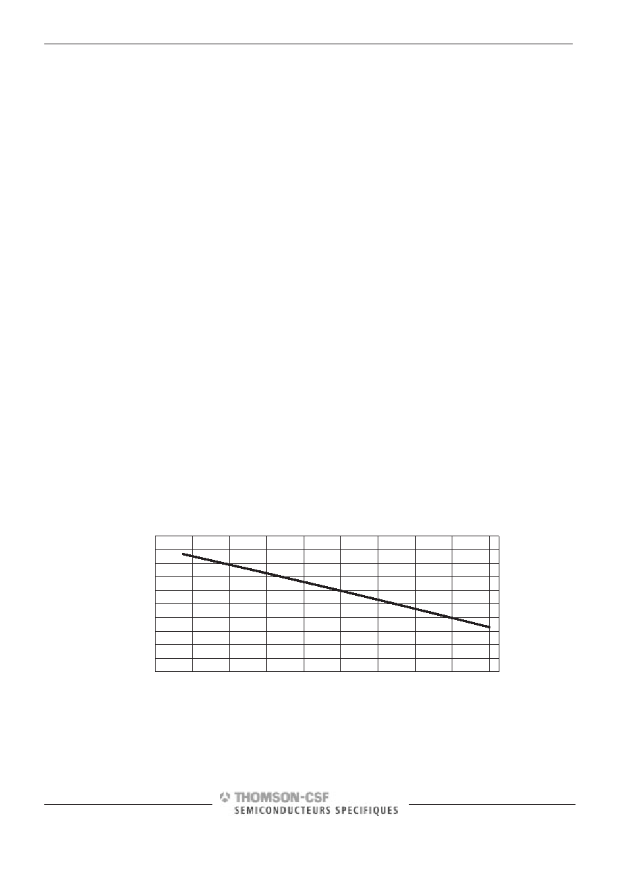
7.10. DIODE PIN K1
One single pin is used for both DRRB input command and die junction monitoring. The pin denomination is DRRB/
DIOD. Temperature monitoring and Data Ready control by DRRB is not possible simultaneously.
(See section 7.2 for Data Ready Reset input command).
The operating die junction temperature must be kept below 145
°C, therefore an adequate cooling system has to be set
up.
The diode mounted transistor measured Vbe value versus junction temperature is given below.
600
640
680
720
760
800
840
880
920
960
1000
–55
–35
–15
5
25
45
65
85
105
125
Junction Temperature (
°C)
VBE (mV)
Idiode = 3mA
相關PDF資料 |
PDF描述 |
|---|---|
| TS8388BCG | 1-CH 8-BIT PROPRIETARY METHOD ADC, PARALLEL ACCESS, CBGA72 |
| TS8388BCG | 1-CH 8-BIT PROPRIETARY METHOD ADC, PARALLEL ACCESS, CBGA72 |
| TS8388BMFB/T | 1-CH 8-BIT PROPRIETARY METHOD ADC, PARALLEL ACCESS, CQFP68 |
| TS8388BMFSB/T | 1-CH 8-BIT PROPRIETARY METHOD ADC, PARALLEL ACCESS, CQFP68 |
| TS8388BMFSB/Q | 1-CH 8-BIT PROPRIETARY METHOD ADC, PARALLEL ACCESS, CQFP68 |
相關代理商/技術參數 |
參數描述 |
|---|---|
| TS8388BCGL | 制造商:e2v technologies 功能描述:ADC 8-BIT 1 GSPS - Trays |
| TS8388BCGL (+LID) | 制造商:e2v technologies 功能描述:ADC 8-BIT 1 GSPS - Trays |
| TS8388BMF | 制造商:e2v technologies 功能描述:ADC 8-BIT 1 GSPS - Trays |
| TS8388BMFB/Q | 制造商:e2v technologies 功能描述:ADC 8-BIT 1 GSPS - Trays |
| TS8388BMFS | 制造商:e2v technologies 功能描述:ADC 8-BIT 1 GSPS - Trays |
發布緊急采購,3分鐘左右您將得到回復。