- 您現(xiàn)在的位置:買賣IC網(wǎng) > PDF目錄98302 > TSC2117IRGZR (TEXAS INSTRUMENTS INC) SPECIALTY CONSUMER CIRCUIT, QCC48 PDF資料下載
參數(shù)資料
| 型號(hào): | TSC2117IRGZR |
| 廠商: | TEXAS INSTRUMENTS INC |
| 元件分類: | 消費(fèi)家電 |
| 英文描述: | SPECIALTY CONSUMER CIRCUIT, QCC48 |
| 封裝: | 7 X 7 MM, GREEN, PLASTIC, VQFN-48 |
| 文件頁(yè)數(shù): | 186/192頁(yè) |
| 文件大小: | 2728K |
| 代理商: | TSC2117IRGZR |
第1頁(yè)第2頁(yè)第3頁(yè)第4頁(yè)第5頁(yè)第6頁(yè)第7頁(yè)第8頁(yè)第9頁(yè)第10頁(yè)第11頁(yè)第12頁(yè)第13頁(yè)第14頁(yè)第15頁(yè)第16頁(yè)第17頁(yè)第18頁(yè)第19頁(yè)第20頁(yè)第21頁(yè)第22頁(yè)第23頁(yè)第24頁(yè)第25頁(yè)第26頁(yè)第27頁(yè)第28頁(yè)第29頁(yè)第30頁(yè)第31頁(yè)第32頁(yè)第33頁(yè)第34頁(yè)第35頁(yè)第36頁(yè)第37頁(yè)第38頁(yè)第39頁(yè)第40頁(yè)第41頁(yè)第42頁(yè)第43頁(yè)第44頁(yè)第45頁(yè)第46頁(yè)第47頁(yè)第48頁(yè)第49頁(yè)第50頁(yè)第51頁(yè)第52頁(yè)第53頁(yè)第54頁(yè)第55頁(yè)第56頁(yè)第57頁(yè)第58頁(yè)第59頁(yè)第60頁(yè)第61頁(yè)第62頁(yè)第63頁(yè)第64頁(yè)第65頁(yè)第66頁(yè)第67頁(yè)第68頁(yè)第69頁(yè)第70頁(yè)第71頁(yè)第72頁(yè)第73頁(yè)第74頁(yè)第75頁(yè)第76頁(yè)第77頁(yè)第78頁(yè)第79頁(yè)第80頁(yè)第81頁(yè)第82頁(yè)第83頁(yè)第84頁(yè)第85頁(yè)第86頁(yè)第87頁(yè)第88頁(yè)第89頁(yè)第90頁(yè)第91頁(yè)第92頁(yè)第93頁(yè)第94頁(yè)第95頁(yè)第96頁(yè)第97頁(yè)第98頁(yè)第99頁(yè)第100頁(yè)第101頁(yè)第102頁(yè)第103頁(yè)第104頁(yè)第105頁(yè)第106頁(yè)第107頁(yè)第108頁(yè)第109頁(yè)第110頁(yè)第111頁(yè)第112頁(yè)第113頁(yè)第114頁(yè)第115頁(yè)第116頁(yè)第117頁(yè)第118頁(yè)第119頁(yè)第120頁(yè)第121頁(yè)第122頁(yè)第123頁(yè)第124頁(yè)第125頁(yè)第126頁(yè)第127頁(yè)第128頁(yè)第129頁(yè)第130頁(yè)第131頁(yè)第132頁(yè)第133頁(yè)第134頁(yè)第135頁(yè)第136頁(yè)第137頁(yè)第138頁(yè)第139頁(yè)第140頁(yè)第141頁(yè)第142頁(yè)第143頁(yè)第144頁(yè)第145頁(yè)第146頁(yè)第147頁(yè)第148頁(yè)第149頁(yè)第150頁(yè)第151頁(yè)第152頁(yè)第153頁(yè)第154頁(yè)第155頁(yè)第156頁(yè)第157頁(yè)第158頁(yè)第159頁(yè)第160頁(yè)第161頁(yè)第162頁(yè)第163頁(yè)第164頁(yè)第165頁(yè)第166頁(yè)第167頁(yè)第168頁(yè)第169頁(yè)第170頁(yè)第171頁(yè)第172頁(yè)第173頁(yè)第174頁(yè)第175頁(yè)第176頁(yè)第177頁(yè)第178頁(yè)第179頁(yè)第180頁(yè)第181頁(yè)第182頁(yè)第183頁(yè)第184頁(yè)第185頁(yè)當(dāng)前第186頁(yè)第187頁(yè)第188頁(yè)第189頁(yè)第190頁(yè)第191頁(yè)第192頁(yè)
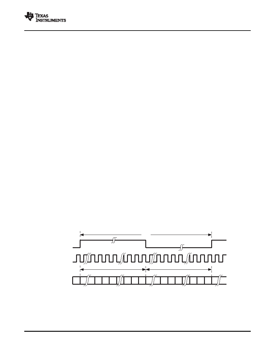
5.9.1.1 Right-Justified Mode
BCLK
WCLK
SDIN/SDOUT
n-1 n-2
1
0
n-1 n-2
1
0
LSB
MSB
LeftChannel
RightChannel
n-3
2
n-3
LSB
MSB
1/fs
TSC2117
Low-Power Audio Codec With Embedded miniDSP, Stereo Class-D
Speaker Amplifier, and Smart Four-Wire Touch-Screen Controller
www.ti.com
SLAS550A – APRIL 2009 – REVISED JUNE 2009
configuring page 0/register 27, D(5:4). In addition, the word clock and bit clock can be independently
configured in either Master or Slave mode, for flexible connectivity to a wide variety of processors. The
word clock is used to define the beginning of a frame, and may be programmed as either a pulse or a
square-wave signal. The frequency of this clock corresponds to the maximum of the selected ADC and
DAC sampling frequencies.
The bit clock is used to clock in and clock out the digital audio data across the serial bus. When in Master
mode, this signal can be programmed to generate variable clock pulses by controlling the bit-clock divider
in page 0/register 30 (see Figure 5-58). The number of bit-clock pulses in a frame may need adjustment to
accommodate various word-lengths as well as to support the case when multiple TSC2117s may share
the same audio bus.
The TSC2117 also includes a feature to offset the position of start of data transfer with respect to the
word-clock. This offset can be controlled in terms of number of bit-clocks and can be programmed in page
0/register 28.
The TSC2117 also has the feature of inverting the polarity of the bit-clock used for transferring the audio
data as compared to the default clock polarity used. This feature can be used independently of the mode
of audio interface chosen. This can be configured via page 0/register 29, D(3).
The TSC2117 further includes programmability (page 0/register 27, D0) to 3-state the SDOUT line during
all bit clocks when valid data is not being sent. By combining this capability with the ability to program at
what bit clock in a frame the audio data begins, time-division multiplexing (TDM) can be accomplished,
enabling the use of multiple codecs on a single audio serial data bus. When the audio serial data bus is
powered down while configured in master mode, the pins associated with the interface are put into a
3-state output condition.
By default when the word-clocks and bit-clocks are generated by the TSC2117, these clocks are active
only when the codec (ADC, DAC or both) are powered up within the device. This is done to save power.
However, it also supports a feature when both the word clocks and bit-clocks can be active even when the
codec in the device is powered down. This is useful when using the TDM mode with multiple codecs on
the same bus, or when word-clock or bit-clocks are used in the system as general-purpose clocks.
The audio interface of the TSC2117 can be put into right-justified mode by programming page 0/register
27, D(7:6) = 10. In right-justified mode, the LSB of the left channel is valid on the rising edge of the bit
clock preceding the falling edge of the word clock. Similarly, the LSB of the right channel is valid on the
rising edge of the bit clock preceding the rising edge of the word clock.
Figure 5-61. Timing Diagram for Right-Justified Mode
For right-justified mode, the number of bit-clocks per frame should be greater than or equal to twice the
programmed word-length of the data.
APPLICATION INFORMATION
93
相關(guān)PDF資料 |
PDF描述 |
|---|---|
| TSC2117IRGZT | SPECIALTY CONSUMER CIRCUIT, QCC48 |
| TSC2300IPAGG4 | SPECIALTY CONSUMER CIRCUIT, PQFP64 |
| TSC2300IPAGR | SPECIALTY CONSUMER CIRCUIT, PQFP64 |
| TSC2300IPAG | SPECIALTY CONSUMER CIRCUIT, PQFP64 |
| TSC2300IPAGRG4 | SPECIALTY CONSUMER CIRCUIT, PQFP64 |
相關(guān)代理商/技術(shù)參數(shù) |
參數(shù)描述 |
|---|---|
| TSC2117IRGZT | 功能描述:觸摸屏轉(zhuǎn)換器和控制器 4-Wire Touch Screen Controller RoHS:否 制造商:Microchip Technology 類型:Resistive Touch Controllers 輸入類型:3 Key 數(shù)據(jù)速率:140 SPS 分辨率:10 bit 接口類型:4-Wire, 5-Wire, 8-Wire, I2C, SPI 電源電壓:2.5 V to 5.25 V 電源電流:17 mA 工作溫度:- 40 C to + 85 C 封裝 / 箱體:SSOP-20 |
| TSC2117IRGZT | 制造商:Texas Instruments 功能描述:Touch Screen Controller IC |
| TSC22 | 制造商:未知廠家 制造商全稱:未知廠家 功能描述:EURO TERMINAL BLOCKS |
| TSC2200 | 制造商:BB 制造商全稱:BB 功能描述:PDA ANALOG INTERFACE CIRCUIT |
| TSC2200EVM | 功能描述:觸摸傳感器開發(fā)工具 Touch Screen Contr Eval Mod RoHS:否 制造商:Cypress Semiconductor 工具用于評(píng)估: 接口類型: 工作電壓: 最大工作溫度: |
發(fā)布緊急采購(gòu),3分鐘左右您將得到回復(fù)。