- 您現在的位置:買賣IC網 > PDF目錄250212 > 70V659S15DR (INTEGRATED DEVICE TECHNOLOGY INC) 128K X 36 DUAL-PORT SRAM, 15 ns, PQFP208 PDF資料下載
參數資料
| 型號: | 70V659S15DR |
| 廠商: | INTEGRATED DEVICE TECHNOLOGY INC |
| 元件分類: | SRAM |
| 英文描述: | 128K X 36 DUAL-PORT SRAM, 15 ns, PQFP208 |
| 封裝: | 28 X 28 MM, 3.50 MM HEIGHT, PLASTIC, QFP-208 |
| 文件頁數: | 5/24頁 |
| 文件大小: | 316K |
| 代理商: | 70V659S15DR |
13
IDT70V659/58/57S
High-Speed 3.3V 128/64/32K x 36 Asynchronous Dual-Port Static RAM
Industrial and Commercial Temperature Ranges
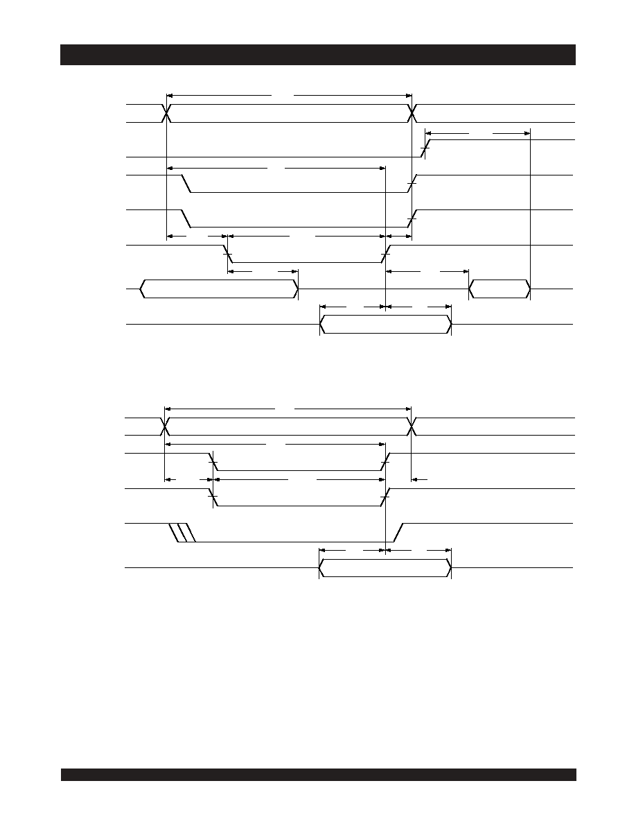
Timing Waveform of Write Cycle No. 1, R/W Controlled Timing(1,5,8)
Timing Waveform of Write Cycle No. 2, CE Controlled Timing(1,5)
NOTES:
1. R/W or CE or BEn = VIH during all address transitions.
2. A write occurs during the overlap (tEW or tWP) of a CE = VIL and a R/W = VIL for memory array writing cycle.
3. tWR is measured from the earlier of CE or R/W (or SEM or R/W) going HIGH to the end of write cycle.
4. During this period, the I/O pins are in the output state and input signals must not be applied.
5. If the CE or SEM = VIL transition occurs simultaneously with or after the R/W = VIL transition, the outputs remain in the High-impedance state.
6. Timing depends on which enable signal is asserted last, CE or R/W.
7. This parameter is guaranteed by device characterization, but is not production tested. Transition is measured 0mV from steady state with the Output Test Load
(Figure 2).
8. If OE = VIL during R/W controlled write cycle, the write pulse width must be the larger of tWP or (tWZ + tDW) to allow the I/O drivers to turn off and data to be
placed on the bus for the required tDW. If OE = VIH during an R/W controlled write cycle, this requirement does not apply and the write pulse can be as short as the
specified tWP.
9. To access RAM, CE = VIL and SEM = VIH. To access semaphore, CE = VIH and SEM = VIL. tEW must be met for either condition.
R/
W
tWC
tHZ
tAW
tWR
tAS
tWP
DATAOUT
(2)
tWZ
tDW
tDH
tOW
OE
ADDRESS
DATAIN
(6)
(4)
(7)
BEn
4869 drw 08
(9)
CE or SEM
(9)
(7)
(3)
4869 drw 09
tWC
tAS
tWR
tDW
tDH
ADDRESS
DATAIN
R/
W
tAW
tEW
BEn
(3)
(2)
(6)
CE or SEM
(9)
相關PDF資料 |
PDF描述 |
|---|---|
| 7P12FLV250I25 | 6M X 16 FLASH 3V PROM CARD, 250 ns, XMA68 |
| 7P12FLV281C15 | 6M X 16 FLASH 3V PROM CARD, 150 ns, XMA68 |
| 7P12FLV512C25 | 6M X 16 FLASH 3V PROM CARD, 250 ns, XMA68 |
| 7P12FLV552I25 | 6M X 16 FLASH 3V PROM CARD, 250 ns, XMA68 |
| 7P12FLV572I15 | 6M X 16 FLASH 3V PROM CARD, 150 ns, XMA68 |
相關代理商/技術參數 |
參數描述 |
|---|---|
| 70V659S15DRI | 制造商:Integrated Device Technology Inc 功能描述:SRAM ASYNC DUAL 3.3V 4.5MBIT 128KX36 15NS 208PQFP - Bulk |
| 70V7319S133BC | 功能描述:IC SRAM 4.5MBIT 133MHZ 256CABGA 制造商:idt, integrated device technology inc 系列:- 包裝:托盤 零件狀態:有效 格式 - 存儲器:RAM 存儲器類型:SRAM - 雙端口,同步 存儲容量:4.5M(256K x 18) 速度:133MHz 接口:并聯 電壓 - 電源:3.15 V ~ 3.45 V 工作溫度:0°C ~ 70°C(TA) 封裝/外殼:256-LBGA 供應商器件封裝:256-CABGA(17x17) 標準包裝:6 |
| 70V7319S133BC8 | 功能描述:IC SRAM 4.5MBIT 133MHZ 256CABGA 制造商:idt, integrated device technology inc 系列:- 包裝:帶卷(TR) 零件狀態:有效 格式 - 存儲器:RAM 存儲器類型:SRAM - 雙端口,同步 存儲容量:4.5M(256K x 18) 速度:133MHz 接口:并聯 電壓 - 電源:3.15 V ~ 3.45 V 工作溫度:0°C ~ 70°C(TA) 封裝/外殼:256-LBGA 供應商器件封裝:256-CABGA(17x17) 標準包裝:1,000 |
| 70V7319S133BF | 功能描述:靜態隨機存取存儲器 RoHS:否 制造商:IDT 存儲容量: 組織: 訪問時間: 電源電壓-最大: 電源電壓-最小: 最大工作電流: 最大工作溫度: 最小工作溫度: 安裝風格: 封裝 / 箱體: 封裝: |
| 70V7319S133BF8 | 制造商:Integrated Device Technology Inc 功能描述:SRAM SYNC DUAL 3.3V 4.5MBIT 256KX18 15NS/4.2NS 208FBGA - Tape and Reel |
發布緊急采購,3分鐘左右您將得到回復。