- 您現(xiàn)在的位置:買賣IC網(wǎng) > PDF目錄36338 > 935262469557 (NXP SEMICONDUCTORS) SPECIALTY CONSUMER CIRCUIT, PQFP240 PDF資料下載
參數(shù)資料
| 型號: | 935262469557 |
| 廠商: | NXP SEMICONDUCTORS |
| 元件分類: | 消費家電 |
| 英文描述: | SPECIALTY CONSUMER CIRCUIT, PQFP240 |
| 封裝: | 32 X 32 MM, 3.40 MM HEIGHT, MSQFP-240 |
| 文件頁數(shù): | 26/518頁 |
| 文件大小: | 7111K |
| 代理商: | 935262469557 |
第1頁第2頁第3頁第4頁第5頁第6頁第7頁第8頁第9頁第10頁第11頁第12頁第13頁第14頁第15頁第16頁第17頁第18頁第19頁第20頁第21頁第22頁第23頁第24頁第25頁當(dāng)前第26頁第27頁第28頁第29頁第30頁第31頁第32頁第33頁第34頁第35頁第36頁第37頁第38頁第39頁第40頁第41頁第42頁第43頁第44頁第45頁第46頁第47頁第48頁第49頁第50頁第51頁第52頁第53頁第54頁第55頁第56頁第57頁第58頁第59頁第60頁第61頁第62頁第63頁第64頁第65頁第66頁第67頁第68頁第69頁第70頁第71頁第72頁第73頁第74頁第75頁第76頁第77頁第78頁第79頁第80頁第81頁第82頁第83頁第84頁第85頁第86頁第87頁第88頁第89頁第90頁第91頁第92頁第93頁第94頁第95頁第96頁第97頁第98頁第99頁第100頁第101頁第102頁第103頁第104頁第105頁第106頁第107頁第108頁第109頁第110頁第111頁第112頁第113頁第114頁第115頁第116頁第117頁第118頁第119頁第120頁第121頁第122頁第123頁第124頁第125頁第126頁第127頁第128頁第129頁第130頁第131頁第132頁第133頁第134頁第135頁第136頁第137頁第138頁第139頁第140頁第141頁第142頁第143頁第144頁第145頁第146頁第147頁第148頁第149頁第150頁第151頁第152頁第153頁第154頁第155頁第156頁第157頁第158頁第159頁第160頁第161頁第162頁第163頁第164頁第165頁第166頁第167頁第168頁第169頁第170頁第171頁第172頁第173頁第174頁第175頁第176頁第177頁第178頁第179頁第180頁第181頁第182頁第183頁第184頁第185頁第186頁第187頁第188頁第189頁第190頁第191頁第192頁第193頁第194頁第195頁第196頁第197頁第198頁第199頁第200頁第201頁第202頁第203頁第204頁第205頁第206頁第207頁第208頁第209頁第210頁第211頁第212頁第213頁第214頁第215頁第216頁第217頁第218頁第219頁第220頁第221頁第222頁第223頁第224頁第225頁第226頁第227頁第228頁第229頁第230頁第231頁第232頁第233頁第234頁第235頁第236頁第237頁第238頁第239頁第240頁第241頁第242頁第243頁第244頁第245頁第246頁第247頁第248頁第249頁第250頁第251頁第252頁第253頁第254頁第255頁第256頁第257頁第258頁第259頁第260頁第261頁第262頁第263頁第264頁第265頁第266頁第267頁第268頁第269頁第270頁第271頁第272頁第273頁第274頁第275頁第276頁第277頁第278頁第279頁第280頁第281頁第282頁第283頁第284頁第285頁第286頁第287頁第288頁第289頁第290頁第291頁第292頁第293頁第294頁第295頁第296頁第297頁第298頁第299頁第300頁第301頁第302頁第303頁第304頁第305頁第306頁第307頁第308頁第309頁第310頁第311頁第312頁第313頁第314頁第315頁第316頁第317頁第318頁第319頁第320頁第321頁第322頁第323頁第324頁第325頁第326頁第327頁第328頁第329頁第330頁第331頁第332頁第333頁第334頁第335頁第336頁第337頁第338頁第339頁第340頁第341頁第342頁第343頁第344頁第345頁第346頁第347頁第348頁第349頁第350頁第351頁第352頁第353頁第354頁第355頁第356頁第357頁第358頁第359頁第360頁第361頁第362頁第363頁第364頁第365頁第366頁第367頁第368頁第369頁第370頁第371頁第372頁第373頁第374頁第375頁第376頁第377頁第378頁第379頁第380頁第381頁第382頁第383頁第384頁第385頁第386頁第387頁第388頁第389頁第390頁第391頁第392頁第393頁第394頁第395頁第396頁第397頁第398頁第399頁第400頁第401頁第402頁第403頁第404頁第405頁第406頁第407頁第408頁第409頁第410頁第411頁第412頁第413頁第414頁第415頁第416頁第417頁第418頁第419頁第420頁第421頁第422頁第423頁第424頁第425頁第426頁第427頁第428頁第429頁第430頁第431頁第432頁第433頁第434頁第435頁第436頁第437頁第438頁第439頁第440頁第441頁第442頁第443頁第444頁第445頁第446頁第447頁第448頁第449頁第450頁第451頁第452頁第453頁第454頁第455頁第456頁第457頁第458頁第459頁第460頁第461頁第462頁第463頁第464頁第465頁第466頁第467頁第468頁第469頁第470頁第471頁第472頁第473頁第474頁第475頁第476頁第477頁第478頁第479頁第480頁第481頁第482頁第483頁第484頁第485頁第486頁第487頁第488頁第489頁第490頁第491頁第492頁第493頁第494頁第495頁第496頁第497頁第498頁第499頁第500頁第501頁第502頁第503頁第504頁第505頁第506頁第507頁第508頁第509頁第510頁第511頁第512頁第513頁第514頁第515頁第516頁第517頁第518頁
Philips Semiconductors
Video Out
File: evo.fm5, modified 7/24/99
PRELIMINARY INFORMATION
7-19
7.14.4
Latency and Bandwidth Requirements
In order to avoid Hardware Bandwidth Errors the internal
highway bus arbiter (see Chapter 19, “Arbiter”) has to be
set accordingly to the latency requirements of VO unit. In
the following all the numbers are given assuming data for
a new video line (Y, U, V and OL (overlay) planar mem-
ory format stored in memory) is aligned to 64 bytes. In
other words, it means {OL,Y,U,V}_OFFSET fields are a
multiple of 64 bytes. Otherwise internal VO arbitration for
OL, Y, U and V requests is changed, and following laten-
cies are not guaranteed. VO uses internal 64 byte buff-
ers.
Latency requirements for VO in image mode 4:2:2 or
4:2:0 co-sited or interspersed without up scaling and
overlay disabled, is expressed as:
During 128 VO clock cycles, VO block requires to
have 2 requests acked ([2 Ys, one U and one V]/2).
If VO clock is 27 MHz then VO has to get two requests
(128 bytes) from SDRAM in 128/.027 = 4740 ns.
Bandwidth (in bytes) requirement per video line within
the active image is:
B1x = [ceil(W/64) + ceil[(W/2)/64]*2 + 4] * 64
ceil(X) function is the least integral value greater than or
equal to X and W is the IMAGE_WIDTH field value.
In the same modes but with overlay enabled the latency
becomes:
During the rst 64 VO clock cycles at least one
request must be acked (the OL data).
During 128 VO clock cycles, VO unit requires to
have 4 requests acked ([4 OLs, 2 Ys, 1 V and 1 U]/2).
If VO clock runs at 54 MHz then VO has to get the first
request from SDRAM in 64/.054 = 1185 ns and average
a bandwidth/latency of 4 requests in 128/.054 = 2370 ns.
Bandwidth (in bytes) per video line within the active im-
age becomes:
B1x,OL = B1x + [ceil(W*2/64) + 4]*64
When VO mode is set to image mode with 2x up scaling
mode the latency requirements are multiplied by a factor
of 2 (i.e. instead of, for example, 1 request per 64 VO
clock cycles, the latency becomes 1 request per 128 VO
clock cycles). Bandwidth is roughly divided by 2:
B2x = (ceil[(W/2)/64] + ceil[((W/2)/2)/64]*2 + 6) * 64
B2x,OL = B2x + (ceil[((W*2)/2)/64] + 4)*64
Latency for raw mode or message passing mode is:
During 64 VO clock cycles, VO block requires to get 1
request from SDRAM.
If VO clock runs at 38 MHz then the latency is 64/.038 =
1684 ns and bandwidth is 38 MB/s.
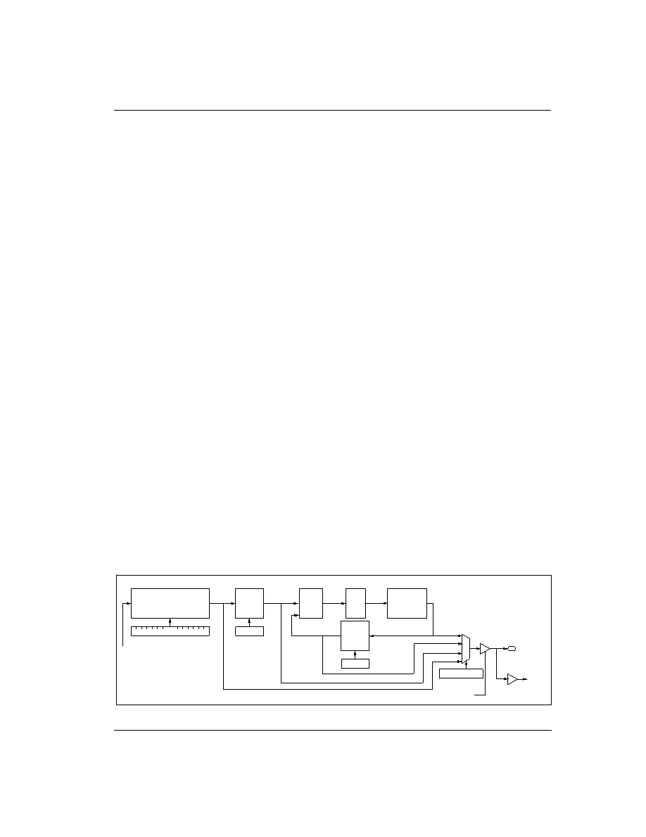
7.15
DDS AND PLL FILTER DETAILS
The PLL filter serves to reduce the phase jitter of the
DDS synthesizer output. It can also be used to multiply
the DDS output frequency by 2x. The DDS and PLL filter
together provide a high quality, accurately programma-
ble output video clock. The complete system is sketched
in Figure 7-27. On hardware reset, the output multiplexer
is set in the ‘11’ position, and the PLL system is disabled.
To start the system, the following steps are needed:
Assign a DDS frequency (this starts the DDS). Allow
for at least 31 DSPCPU cycles for the DDS fre-
quency setting to take effect.
Choose a value for PLL_S, PLL_T (for 8-40 MHz
operation, a value of 1 for division by 2 is recom-
mended).
Choose a value for CLOCK_SELECT (for 8-80 MHz
operation, CLOCK_SELECT=00 is recommended).
Assign a VO_CTL word containing the above
choices. The rst assignment with CLOCK_SELECT
unequal 11 enables the PLL system. Allow for max.
50 microseconds to achieve lock.
Once the PLL is locked, small changes to the DDS fre-
quency are allowed, and the VO_CLK output will
smoothly track the frequency change.
Note that most consumer electronics equipment impos-
es
very high precision requirements on the value of the
color burst frequency. A video encoder derives the color
burst frequency from VO_CLK. In the case of changing
the VO_CLK frequency to software phase lock to a mas-
ter reference, special care is required to keep the color
burst signal frequency within a tolerance of some 50
00
01
10
11
Square-Wave DDS
FREQUENCY
VCO
8 - 90 MHz
VO_CLK
VO_CLK Internal
(to Frame Timing Gen.)
CLKOUT
3
× CPU Clock
0
3
Loop
Filter
Phase
Detect
PLL_S
div T+1
PLL_T
CLOCK_SELECT
div S+1
Figure 7-27. PLL filter block diagram
相關(guān)PDF資料 |
PDF描述 |
|---|---|
| 935263151557 | SPECIALTY CONSUMER CIRCUIT, PQFP240 |
| 935263331557 | SPECIALTY CONSUMER CIRCUIT, PQFP240 |
| 935263133112 | 26 W, 1 CHANNEL, AUDIO AMPLIFIER, PZIP17 |
| 935263384118 | SPECIALTY ANALOG CIRCUIT, PDSO16 |
| 935263384112 | SPECIALTY ANALOG CIRCUIT, PDSO16 |
相關(guān)代理商/技術(shù)參數(shù) |
參數(shù)描述 |
|---|---|
| 935264217557 | 制造商:NXP Semiconductors 功能描述:SUB ONLY IC |
| 935267356112 | 制造商:NXP Semiconductors 功能描述:IC TEA1507PN |
| 935268081112 | 制造商:NXP Semiconductors 功能描述:SUB ONLY IC |
| 935268721125 | 制造商:NXP Semiconductors 功能描述:Buffer/Line Driver 1-CH Non-Inverting 3-ST CMOS 5-Pin TSSOP T/R |
| 935269304128 | 制造商:ST-Ericsson 功能描述:IC AUDIO CODEC W/TCH SCRN 48LQFP |
發(fā)布緊急采購,3分鐘左右您將得到回復(fù)。