- 您現(xiàn)在的位置:買賣IC網(wǎng) > PDF目錄373915 > AD7725 (Analog Devices, Inc.) 16-Bit 900 kSPS ADC with a Programmable Postprocessor PDF資料下載
參數(shù)資料
| 型號: | AD7725 |
| 廠商: | Analog Devices, Inc. |
| 英文描述: | 16-Bit 900 kSPS ADC with a Programmable Postprocessor |
| 中文描述: | 16位900 ksps模數(shù)轉(zhuǎn)換器的可編程后處理器 |
| 文件頁數(shù): | 25/28頁 |
| 文件大小: | 442K |
| 代理商: | AD7725 |
第1頁第2頁第3頁第4頁第5頁第6頁第7頁第8頁第9頁第10頁第11頁第12頁第13頁第14頁第15頁第16頁第17頁第18頁第19頁第20頁第21頁第22頁第23頁第24頁當(dāng)前第25頁第26頁第27頁第28頁
REV. A
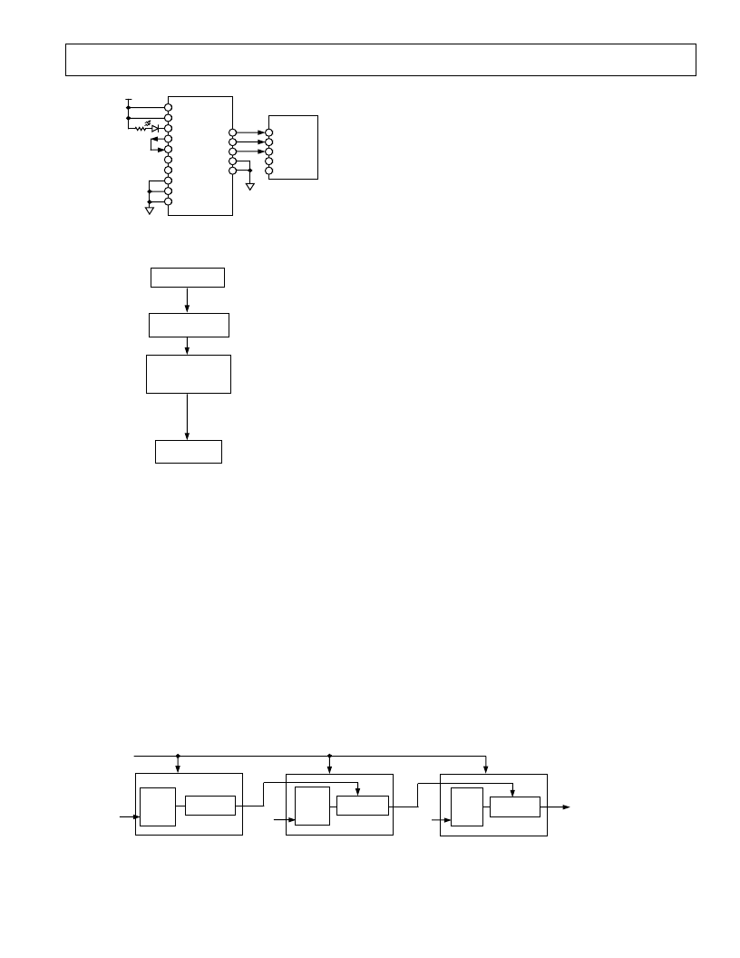
AD7725
–25–
DV
DD
SOE
SMODE0
SMODE1
SYNC
ERR
CFGEND
DVAL
S/
P
RESETCFG
INIT
SCO
FSO
SDO
SDI
FSI
AD7725
SCLK0
RFS0
DR0
DT0
TFS0
ADSP-21xx
Figure 30. Connection Diagram for Loading the
Default Filter in BFR Mode
POWER-ON RESET
IMMEDIATE BOOT
FROM ROM
DEFAULTFILTER
LOADED INTO
POSTPROCESSOR
FROM INTERNAL ROM
CFGEND = 1
INIT = 1
DEVICE STARTS
CONVERTING
SMODE0 = 0
SMODE1 = 0
Figure 31. Flow Chart of BFR Mode
DAISY-CHAINING DEVICES
Several AD7725s can be daisy-chained/cascaded together.
This feature of the AD7725 reduces system demands as it
allows several devices to be configured using one serial data
stream. It also allows conversion data from several devices to
be read back by a single DSP as one serial data stream. When
devices are daisy-chained, configuration/conversion data flows
from device to device using the SDO/FSO and SDI/FSI pins of
each device. A specific daisy-chaining configuration file needs
to be developed using the filter design package Filter Wizard.
The following sections describe the daisy-chaining options the
user can choose.
Daisy-Chaining during Configuration
Several AD7725s can be daisy-chained together so that they can
all be configured from a common external serial EPROM or a
DSP. Filter Wizard allows the user to specify the number of
devices in the chain and to design a specific filter for each device.
It then generates a separate configuration file for each device.
The configuration files for all the devices can be combined
into one configuration file in order, starting with the file for
the first device, (for example, with a text editor) so that the
user only has to load one file into the EPROM or DSP. This
configuration file is loaded into the devices using the FSI/SDI
and the FSO/SDO of each device. Once the devices have been
configured in a daisy chain, each device can be run indepen-
dently, and conversion data is read back using the FSO and
SDO from each device separately.
Daisy-Chaining—Configuration and Conversion Data
Several AD7725s can be daisy-chained so that they are con-
figured from a common external serial EPROM or DSP (as
discussed earlier in Daisy-Chaining during Configuration),
and all conversion data from each individual device can be
read back by a single DSP on one serial data stream. To do
this, an interlacer is required following each filter on each
device. This design can be implemented using Filter Wizard.
The function of the interlacer is to sequentially combine the
conversion data outputs of each device into one serial data
stream. The interlacer combines the data using interpolation
and summing. Interpolation pads the data with zeros; then the
interlacer takes the output data from the previous device, delays
it by one clock cycle and sums it with the interpolated output
from the current device. This occurs on each device in the chain,
and the output data from the last device consists of the conver-
sion data from all devices in one continuous data stream. When
designing filters with interlacing, the decimation rate of the filter
on each device should be twice the number of devices in the
chain, or a multiple of this value, to ensure there is no interfer-
ence between the conversion data of different devices. Due to
the interpolation and decimation, the effective output data rate
of each device (out of the last device) is CLKIN/(16 number
of devices) and the actual output data rate of the final device is
CLKIN/16. Once the daisy-chaining and interlacing design is
complete, one configuration file is generated to be loaded into
the devices. Figure 32 shows an example of daisy-chaining three
devices, using interlacing.
Loading Configuration Data
When loading the configuration file from a common EPROM or
DSP, the configuration data is loaded into the first device in the
chain. Once this device is configured, the data will be loaded
into the second device in the chain via FSO/SDO of Device 1
and FSI/SDI of Device 2. When this device is configured,
the data is loaded into the next device in the chain until all
devices are configured. The CFGEND pin of the last device is
connected to the INIT pin of all the devices so that when the
last device is successfully configured, conversions are initiated.
DEVICE1
DEVICE3
DEVICE2
ANALOG
INPUT
ANALOG
INPUT
FILTER1
DEC 6
FILTER2
DEC 6
FILTER3
DEC 6
DIGITAL
INPUT
DIGITAL
INPUT
INTERLACER
INTERLACER
INTERLACER
DATA OUTPUT FORMAT:
DEVICE3, DEVICE2,
DEVICE1; DEVICE3, ...
EFFECTIVE DATA OUTPUT RATE
FROM EACH DEVICE:
= CLKIN/(16 3)
= 200kSPS
DATA OUTPUT
RATE = CLKIN/16
ANALOG
INPUT
CLKIN
9.6MHz
Figure 32. Daisy-Chaining Example
相關(guān)PDF資料 |
PDF描述 |
|---|---|
| AD7725BS | 16-Bit 900 kSPS ADC with a Programmable Postprocessor |
| AD7729 | Dual Sigma-Delta ADC with Auxiliary DAC |
| AD7729AR | Dual Sigma-Delta ADC with Auxiliary DAC |
| AD7729ARU | Dual Sigma-Delta ADC with Auxiliary DAC |
| AD7730LBR | Bridge Transducer ADC |
相關(guān)代理商/技術(shù)參數(shù) |
參數(shù)描述 |
|---|---|
| AD7725BS | 制造商:Analog Devices 功能描述:ADC Single Delta-Sigma 900ksps 16-bit Parallel/Serial 44-Pin MQFP 制造商:Rochester Electronics LLC 功能描述:16-BIT PROGRAMMABLE SIGMA-DELTA ADC I.C. - Bulk 制造商:Analog Devices 功能描述:IC 16BIT ADC SMD 7725 MQFP44 |
| AD7725BSC-REEL | 制造商:Analog Devices 功能描述: |
| AD7725BS-REEL | 制造商:Analog Devices 功能描述:ADC Single Delta-Sigma 900ksps 16-bit Parallel/Serial 44-Pin MQFP T/R 制造商:Rochester Electronics LLC 功能描述:16-BIT PROGRAMMABLE SIGMA-DELTA ADC I.C. - Tape and Reel |
| AD7725BSZ | 功能描述:IC ADC 16BIT PROG 44MQFP RoHS:是 類別:集成電路 (IC) >> 數(shù)據(jù)采集 - 模數(shù)轉(zhuǎn)換器 系列:- 產(chǎn)品培訓(xùn)模塊:Lead (SnPb) Finish for COTS Obsolescence Mitigation Program 標(biāo)準(zhǔn)包裝:2,500 系列:- 位數(shù):12 采樣率(每秒):3M 數(shù)據(jù)接口:- 轉(zhuǎn)換器數(shù)目:- 功率耗散(最大):- 電壓電源:- 工作溫度:- 安裝類型:表面貼裝 封裝/外殼:SOT-23-6 供應(yīng)商設(shè)備封裝:SOT-23-6 包裝:帶卷 (TR) 輸入數(shù)目和類型:- |
| AD7727BCPZRL | 制造商:Analog Devices 功能描述: |
發(fā)布緊急采購,3分鐘左右您將得到回復(fù)。