- 您現在的位置:買賣IC網 > PDF目錄373915 > AD7725 (Analog Devices, Inc.) 16-Bit 900 kSPS ADC with a Programmable Postprocessor PDF資料下載
參數資料
| 型號: | AD7725 |
| 廠商: | Analog Devices, Inc. |
| 英文描述: | 16-Bit 900 kSPS ADC with a Programmable Postprocessor |
| 中文描述: | 16位900 ksps模數轉換器的可編程后處理器 |
| 文件頁數: | 8/28頁 |
| 文件大小: | 442K |
| 代理商: | AD7725 |
第1頁第2頁第3頁第4頁第5頁第6頁第7頁當前第8頁第9頁第10頁第11頁第12頁第13頁第14頁第15頁第16頁第17頁第18頁第19頁第20頁第21頁第22頁第23頁第24頁第25頁第26頁第27頁第28頁
REV. A
–8–
AD7725
ABSOLUTE MAXIMUM RATINGS
1
(T
A
= 25
°
C, unless otherwise noted.)
DV
DD
to DGND . . . . . . . . . . . . . . . . . . . . . . . . –0.3 V to +7 V
AV
DD
to AGND . . . . . . . . . . . . . . . . . . . . . . . . . –0.3 V to +7 V
AV
DD
, AV
DD1
to DV
DD
. . . . . . . . . . . . . . . . . . . . –1 V to +1 V
AGND, AGND1 to DGND . . . . . . . . . . . . . –0.3 V to +0.3 V
Digital Inputs to DGND . . . . . . . . . . –0.3 V to DV
DD
+ 0.3 V
Digital Outputs to DGND . . . . . . . . . –0.3 V to DV
DD
+ 0.3 V
V
IN
(+), V
IN
(–) to AGND . . . . . . . . . . .–0.3 V to AV
DD
+ 0.3 V
REF1 to AGND . . . . . . . . . . . . . . . . .–0.3 V to AV
DD
+ 0.3 V
REF2 to AGND . . . . . . . . . . . . . . . . .–0.3 V to AV
DD
+ 0.3 V
REFIN to AGND . . . . . . . . . . . . . . . .–0.3 V to AV
DD
+ 0.3 V
DGND, AGND . . . . . . . . . . . . . . . . . . . . . . . . . . . . . . .
±
0.3 V
Input Current to Any Pin except Supplies
2
. . . . . . . . .
±
10 mA
I
DD
(AI
DD
+ DI
DD
) . . . . . . . . . . . . . . . . . . . . . . . . . . . . 150 mA
Operating Temperature Range . . . . . . . . . . . .–40
°
C to +85
°
C
Storage Temperature Range . . . . . . . . . . . . .–65
°
C to +150
°
C
Junction Temperature . . . . . . . . . . . . . . . . . . . . . . . . . . 150
°
C
JA
Thermal Impedance . . . . . . . . . . . . . . . . . . . . . . . . 58
°
C/W
JC
Thermal Impedance . . . . . . . . . . . . . . . . . . . . . . . . 20
°
C/W
Lead Temperature, Soldering
Vapor Phase (60 sec) . . . . . . . . . . . . . . . . . . . . . . . . . 215
°
C
Infrared (15 sec) . . . . . . . . . . . . . . . . . . . . . . . . . . . . 220
°
C
ESD . . . . . . . . . . . . . . . . . . . . . . . . . . . . . . . . . . . . . . . . . .2 kV
NOTES
1
Stresses above those listed under Absolute Maximum Ratings may cause perma-
nent damage to the device. This is a stress rating only; functional operation of the
device at these or any other conditions above those indicated in the operational
section of this specification is not implied. Exposure to absolute maximum rating
conditions for extended periods may affect device reliability.
2
Transient currents of up to 100 mA will not cause SCR latch-up.
CAUTION
ESD (electrostatic discharge) sensitive device. Electrostatic charges as high as 4000 V readily
accumulate on the human body and test equipment and can discharge without detection. Although the
AD7725 features proprietary ESD protection circuitry, permanent damage may occur on devices
subjected to high energy electrostatic discharges. Therefore, proper ESD precautions are recommended
to avoid performance degradation or loss of functionality.
ORDERING GUIDE
Temperature
Range
Package
Description
Package
Option
1
Model
AD7725BS
–40
°
C to +85
°
C
Metric Quad
Flatpack
S-44-2
AD7725BS-REEL –40
°
C to +85
°
C
Metric Quad
Flatpack
S-44-2
EVAL-
AD7725CB
2
Evaluation
Board
EVAL-
CONTROL
BRD2
3
Controller
Board
NOTES
1
S = Metric Quad Flat Package (MQFP).
2
This board can be used as a standalone evaluation board or in conjunction with the
Evaluation Board Controller for evaluation/demonstration purposes. It is accom-
panied by software and technical documentation.
3
Evaluation Board Controller. This board is a complete unit allowing a PC to
control and communicate with all Analog Devices boards ending in the CB
designator. To obtain the complete evaluation kit, the following needs to be
ordered: EVAL-AD7725CB, EVAL-CONTROL BRD2, and a 12 V ac transformer.
The Filter Wizard software can be downloaded from the Analog Devices website.
S
T
A
T
U
S
I
N
S
T
RUC
T
I
ON
DB0 DB15
–
INT
RS
CS
RD/
WR
t
34
t
33
t
40
t
36
t
35
t
38
t
23
t
37
t
39
THREE-STATE
THREE-STATE
THREE-STATE
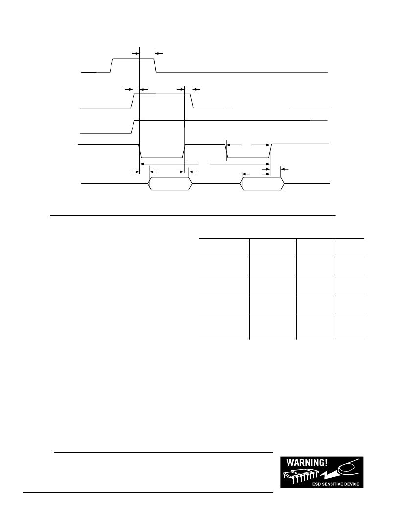
Figure 8. Parallel Mode (Reading the Status Register and Writing Instructions)
相關PDF資料 |
PDF描述 |
|---|---|
| AD7725BS | 16-Bit 900 kSPS ADC with a Programmable Postprocessor |
| AD7729 | Dual Sigma-Delta ADC with Auxiliary DAC |
| AD7729AR | Dual Sigma-Delta ADC with Auxiliary DAC |
| AD7729ARU | Dual Sigma-Delta ADC with Auxiliary DAC |
| AD7730LBR | Bridge Transducer ADC |
相關代理商/技術參數 |
參數描述 |
|---|---|
| AD7725BS | 制造商:Analog Devices 功能描述:ADC Single Delta-Sigma 900ksps 16-bit Parallel/Serial 44-Pin MQFP 制造商:Rochester Electronics LLC 功能描述:16-BIT PROGRAMMABLE SIGMA-DELTA ADC I.C. - Bulk 制造商:Analog Devices 功能描述:IC 16BIT ADC SMD 7725 MQFP44 |
| AD7725BSC-REEL | 制造商:Analog Devices 功能描述: |
| AD7725BS-REEL | 制造商:Analog Devices 功能描述:ADC Single Delta-Sigma 900ksps 16-bit Parallel/Serial 44-Pin MQFP T/R 制造商:Rochester Electronics LLC 功能描述:16-BIT PROGRAMMABLE SIGMA-DELTA ADC I.C. - Tape and Reel |
| AD7725BSZ | 功能描述:IC ADC 16BIT PROG 44MQFP RoHS:是 類別:集成電路 (IC) >> 數據采集 - 模數轉換器 系列:- 產品培訓模塊:Lead (SnPb) Finish for COTS Obsolescence Mitigation Program 標準包裝:2,500 系列:- 位數:12 采樣率(每秒):3M 數據接口:- 轉換器數目:- 功率耗散(最大):- 電壓電源:- 工作溫度:- 安裝類型:表面貼裝 封裝/外殼:SOT-23-6 供應商設備封裝:SOT-23-6 包裝:帶卷 (TR) 輸入數目和類型:- |
| AD7727BCPZRL | 制造商:Analog Devices 功能描述: |
發布緊急采購,3分鐘左右您將得到回復。