- 您現在的位置:買賣IC網 > PDF目錄373915 > AD7725 (Analog Devices, Inc.) 16-Bit 900 kSPS ADC with a Programmable Postprocessor PDF資料下載
參數資料
| 型號: | AD7725 |
| 廠商: | Analog Devices, Inc. |
| 英文描述: | 16-Bit 900 kSPS ADC with a Programmable Postprocessor |
| 中文描述: | 16位900 ksps模數轉換器的可編程后處理器 |
| 文件頁數: | 27/28頁 |
| 文件大小: | 442K |
| 代理商: | AD7725 |
第1頁第2頁第3頁第4頁第5頁第6頁第7頁第8頁第9頁第10頁第11頁第12頁第13頁第14頁第15頁第16頁第17頁第18頁第19頁第20頁第21頁第22頁第23頁第24頁第25頁第26頁當前第27頁第28頁
REV. A
AD7725
–27–
A minimum etch technique is generally best for ground planes
as it gives the best shielding. Noise can be minimized by paying
attention to the system layout and preventing different signals
from interfering with each other. High level analog signals should
be separated from low level analog signals, and both should be
kept away from digital signals. In waveform sampling and recon-
struction systems, the sampling clock (CLKIN) is as vulnerable
to noise as any analog signal. CLKIN should be isolated from the
analog and digital systems. Fast switching signals like clocks
should be shielded with their associated ground to avoid radiating
noise to other sections of the board, and clock signals should
never be routed near the analog inputs.
Avoid running digital lines under the device, as these will couple
noise onto the die. The analog ground plane should be allowed
to run under the AD7725 to shield it from noise coupling. The
power supply lines to the AD7725 should use as large a trace as
possible (preferably a plane) to provide a low impedance path
and reduce the effects of glitches on the power supply line.
Avoid crossover of digital and analog signals. Traces on oppo-
site sides of the board should run at right angles to each other.
This will reduce the effects of feedthrough through the board.
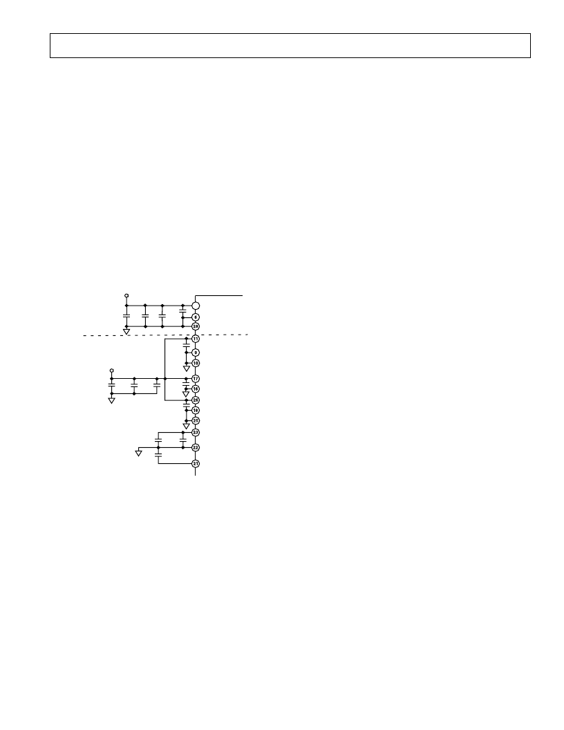
0.1 F
AV
DD
AGND
10nF
DV
DD
DGND
DGND
5V
DGND
10 F+
10nF
10nF
10nF
AV
DD
1
AGND1
AGND1
AV
DD
AGND
10nF
AGND
0.1 F
0.1 F
10 F
5V
AGND
REF2
REF1
AGND2
220nF
10nF
1 F
ANALOG
GROUND
PLANE
DIGITAL
GROUND
PLANE
39
Figure 36. Reference and Supply Decoupling
OPTIMIZING HEAT REMOVAL BY PCB
CONSTRUCTION AND DEVICE MOUNTING
For normal still air conditions, the primary heat dissipation path
from the chip to the ambient is via the component leads into the
PCB. The thermal resistance of the board is then a significant
variable. This can be lowered by maximizing the use of ground
planes as heat sinks and also by optimizing the way in which the
heat can be dissipated, for example conduction into the board
mounting chassis. The greater the percentage of copper in the
board, especially in the region of the device, the lower the ther-
mal resistance. The use of wide tracks and thermal vias to the
ground plane will have a significant effect. Placing critical com-
ponents close to where the edge of the board is attached to the
chassis can provide additional cooling without the use of heat
sinks or forced air. Avoid close spacing of high power devices in
order to ensure that the heat is dissipated over the maximum
possible area.
EVALUATING THE AD7725 PERFORMANCE
There is an AD7725 evaluation package available that includes
a fully assembled and tested evaluation board, documentation,
and software for controlling the board from a PC via the Evalu-
ation Board Controller. The Evaluation Board Controller can
be used in conjunction with the AD7725 Evaluation Board (as
well as with many other Analog Devices evaluation boards ending
in the CB designator) to demonstrate/evaluate the performance of
the AD7725. The software allows the user to perform ac (Fast
Fourier Transform) and dc (Histogram of Codes) tests on the
AD7725. By downloading the filter design package, Filter
Wizard, user-defined filter files can be loaded into the AD7725
to program the postprocessor via the Evaluation Board Controller.
See the ADI website for more information.
相關PDF資料 |
PDF描述 |
|---|---|
| AD7725BS | 16-Bit 900 kSPS ADC with a Programmable Postprocessor |
| AD7729 | Dual Sigma-Delta ADC with Auxiliary DAC |
| AD7729AR | Dual Sigma-Delta ADC with Auxiliary DAC |
| AD7729ARU | Dual Sigma-Delta ADC with Auxiliary DAC |
| AD7730LBR | Bridge Transducer ADC |
相關代理商/技術參數 |
參數描述 |
|---|---|
| AD7725BS | 制造商:Analog Devices 功能描述:ADC Single Delta-Sigma 900ksps 16-bit Parallel/Serial 44-Pin MQFP 制造商:Rochester Electronics LLC 功能描述:16-BIT PROGRAMMABLE SIGMA-DELTA ADC I.C. - Bulk 制造商:Analog Devices 功能描述:IC 16BIT ADC SMD 7725 MQFP44 |
| AD7725BSC-REEL | 制造商:Analog Devices 功能描述: |
| AD7725BS-REEL | 制造商:Analog Devices 功能描述:ADC Single Delta-Sigma 900ksps 16-bit Parallel/Serial 44-Pin MQFP T/R 制造商:Rochester Electronics LLC 功能描述:16-BIT PROGRAMMABLE SIGMA-DELTA ADC I.C. - Tape and Reel |
| AD7725BSZ | 功能描述:IC ADC 16BIT PROG 44MQFP RoHS:是 類別:集成電路 (IC) >> 數據采集 - 模數轉換器 系列:- 產品培訓模塊:Lead (SnPb) Finish for COTS Obsolescence Mitigation Program 標準包裝:2,500 系列:- 位數:12 采樣率(每秒):3M 數據接口:- 轉換器數目:- 功率耗散(最大):- 電壓電源:- 工作溫度:- 安裝類型:表面貼裝 封裝/外殼:SOT-23-6 供應商設備封裝:SOT-23-6 包裝:帶卷 (TR) 輸入數目和類型:- |
| AD7727BCPZRL | 制造商:Analog Devices 功能描述: |
發布緊急采購,3分鐘左右您將得到回復。