- 您現在的位置:買賣IC網 > PDF目錄373970 > AD9910_07 (Analog Devices, Inc.) 1 GSPS, 14-Bit, 3.3 V CMOS Direct Digital Synthesizer PDF資料下載
參數資料
| 型號: | AD9910_07 |
| 廠商: | Analog Devices, Inc. |
| 元件分類: | XO, clock |
| 英文描述: | 1 GSPS, 14-Bit, 3.3 V CMOS Direct Digital Synthesizer |
| 中文描述: | 1 GSPS的,14位,3.3伏的CMOS直接數字頻率合成 |
| 文件頁數: | 33/60頁 |
| 文件大小: | 764K |
| 代理商: | AD9910_07 |
第1頁第2頁第3頁第4頁第5頁第6頁第7頁第8頁第9頁第10頁第11頁第12頁第13頁第14頁第15頁第16頁第17頁第18頁第19頁第20頁第21頁第22頁第23頁第24頁第25頁第26頁第27頁第28頁第29頁第30頁第31頁第32頁當前第33頁第34頁第35頁第36頁第37頁第38頁第39頁第40頁第41頁第42頁第43頁第44頁第45頁第46頁第47頁第48頁第49頁第50頁第51頁第52頁第53頁第54頁第55頁第56頁第57頁第58頁第59頁第60頁
AD9910
Rev. 0 | Page 33 of 60
RAM
A
D
Q
PROFILE
DDS CLOCK
RAM
PROFILE
REGISTERS
STATE
MACHINE
UP/DOWN
COUNTER
32
10
2
3
16
10
10
U/D
3
0
WAVEFORM END ADDRESS
ADDRESS RAMP RATE
WAVEFORM START ADDRESS
NO DWELL
RAM MODE
TO DDS
SIGNAL
CONTROL
PARAMETER
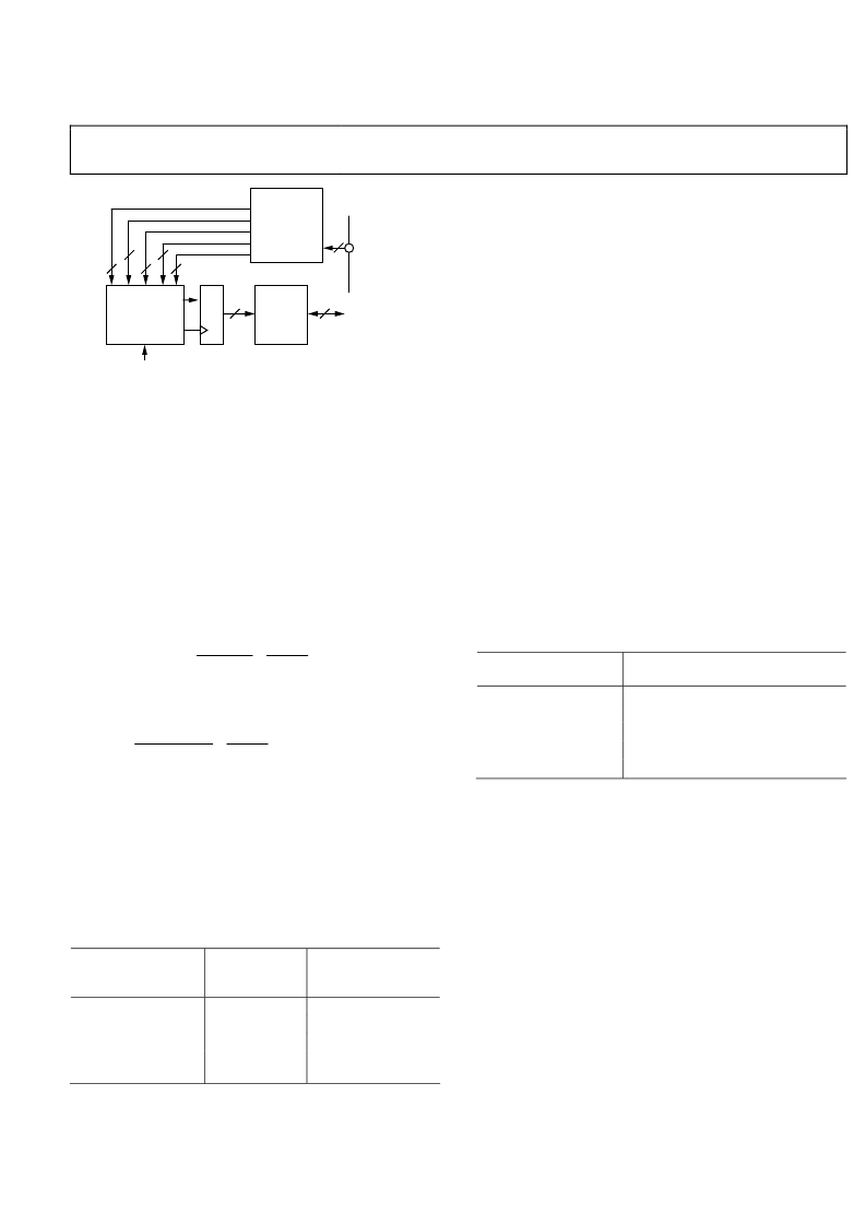
Figure 42. RAM Playback Operation
During playback, the state machine uses an up/down counter to
step through the specified address locations. The clock rate of
this counter defines the playback rate; that is, the sample rate of
the generated waveform. The clocking of the counter is
controlled by a 16-bit programmable timer that is internal to
the state machine. This timer is clocked by the DDS clock and
its time interval is set by the 16-bit address step rate value
stored in the selected RAM profile register.
The address step rate value determines the playback rate. For
example, if M is the 16-bit value of the address step rate for a
specific RAM profile, then the playback rate for that profile is
given by
f
Rate
Playback
=
M
f
M
SYSCLK
4
DDSCLOCK
=
The sample interval (Δt) associated with the playback rate, is
therefore given by
M
Rate
Playback
SYSCLK
f
t
4
1
Δ
=
=
RAM data entry/retrieval via the I/O port takes precedence
over playback operation. An I/O operation targeting the RAM
during playback interrupts any waveform in progress.
The 32-bit words output by the RAM during playback route to
the DDS signal control parameters according to two RAM
Playback Destination bits in Control Function Register 1. The
32-bit words are partitioned based on Table 12.
Table 12. RAM Playback Destination
RAM Playback
Destination Bits
CFR1<30:29>
00
01
10
11
DDS Signal
Control
Parameter
Frequency
Phase
Amplitude
Polar (phase
and amplitude)
Bits Assigned to
DDS Parameters
31:0
31:16
31:18
Phase<31:16>
Amplitude<15:2>
When the destination is phase, amplitude, or polar the unused
LSBs are ignored.
The RAM playback destination bits affect specific DDS signal
control parameters. The parameters that are not affected by the
RAM playback destination bits are controlled by the FTW POW
and/or ASF registers.
RAM_SWP_OVR (RAM Sweep Over) Pin
The RAM_SWP_OVR pin provides an active high external
signal that indicates the end of a playback sequence. The
operation of this pin varies with the RAM operating mode
as detailed in the following sections. When RAM enable = 0,
this pin is forced to a Logic 0.
Overview of RAM Playback Modes
The RAM can operate in any one of five different playback modes:
Direct switch
Ramp up
Bidirectional ramp
Continuous bidirectional ramp
Continuous recirculate
The mode is selected via the 3-bit RAM mode control word
located in each of the RAM profile registers. Thus, the RAM
operating mode is profile dependent. The RAM profile mode
control bits are detailed in Table 13.
Table 13. RAM Operating Modes
RAM Profile
Mode Control Bits
000, 101, 110, 111
001
010
011
100
RAM Operating Mode
Direct switch
Ramp up
Bidirectional ramp
Continuous bidirectional ramp
Continuous recirculate
RAM Direct Switch Mode
In direct switch mode, the RAM is not used as a waveform
generator. Instead, when a RAM profile is selected via the
PROFILE pins only a single 32-bit word is routed to the DDS to
be applied to the signal control parameter(s). This 32-bit word
is the data stored in the RAM at the location given by the 10-bit
waveform start address of the selected profile.
In direct switch mode, the RAM_SWP_OVR pin is always
Logic 0 and the no-dwell high bit is ignored.
Direct switch mode enables up to eight-level FSK, PSK, or ASK
modulation; the type of modulation is determined by the RAM
playback destination bits (frequency for FSK, and so on). Each
RAM profile is associated with a specific value of frequency,
phase, or amplitude. Each unique waveform start address value
in each RAM profile allows access of the 32-bit word stored in
that particular RAM location. In this way, the profile pins
implement the shift-keying function, modulating the DDS
output as desired.
相關PDF資料 |
PDF描述 |
|---|---|
| AD9910BSVZ | 1 GSPS, 14-Bit, 3.3 V CMOS Direct Digital Synthesizer |
| AD9910BSVZ-REEL | 1 GSPS, 14-Bit, 3.3 V CMOS Direct Digital Synthesizer |
| AD9912 | 1 GSPS Direct Digital Synthesizer w/ 14-bit DAC |
| AD9913 | Low Power 250 MSPS 10-Bit DAC 1.8 V CMOS Direct Digital Synthesizer |
| AD9913BCPZ1 | Low Power 250 MSPS 10-Bit DAC 1.8 V CMOS Direct Digital Synthesizer |
相關代理商/技術參數 |
參數描述 |
|---|---|
| AD9910BSVZ | 功能描述:IC DDS 1GSPS 14BIT PAR 100TQFP RoHS:是 類別:集成電路 (IC) >> 接口 - 直接數字合成 (DDS) 系列:- 產品變化通告:Product Discontinuance 27/Oct/2011 標準包裝:2,500 系列:- 分辨率(位):10 b 主 fclk:25MHz 調節字寬(位):32 b 電源電壓:2.97 V ~ 5.5 V 工作溫度:-40°C ~ 85°C 安裝類型:表面貼裝 封裝/外殼:16-TSSOP(0.173",4.40mm 寬) 供應商設備封裝:16-TSSOP 包裝:帶卷 (TR) |
| AD9910BSVZ | 制造商:Analog Devices 功能描述:IC DDS 1GHZ TQFP-100 制造商:Analog Devices 功能描述:IC, DDS, 1GHZ, TQFP-100 |
| AD9910BSVZ-REEL | 功能描述:IC DDS 1GSPS 14BIT PAR 100TQFP RoHS:是 類別:集成電路 (IC) >> 接口 - 直接數字合成 (DDS) 系列:- 產品變化通告:Product Discontinuance 27/Oct/2011 標準包裝:2,500 系列:- 分辨率(位):10 b 主 fclk:25MHz 調節字寬(位):32 b 電源電壓:2.97 V ~ 5.5 V 工作溫度:-40°C ~ 85°C 安裝類型:表面貼裝 封裝/外殼:16-TSSOP(0.173",4.40mm 寬) 供應商設備封裝:16-TSSOP 包裝:帶卷 (TR) |
| AD9911 | 制造商:AD 制造商全稱:Analog Devices 功能描述:500 MSPS Direct Digital Synthesizer with 10-Bit DAC |
| AD9911/PCB | 制造商:Analog Devices 功能描述:500 MSPS DIRECT DGTL SYNTHESIZER W/ 10-BIT DAC AD9911/PCB - Bulk |
發布緊急采購,3分鐘左右您將得到回復。