- 您現在的位置:買賣IC網 > PDF目錄373970 > AD9910_07 (Analog Devices, Inc.) 1 GSPS, 14-Bit, 3.3 V CMOS Direct Digital Synthesizer PDF資料下載
參數資料
| 型號: | AD9910_07 |
| 廠商: | Analog Devices, Inc. |
| 元件分類: | XO, clock |
| 英文描述: | 1 GSPS, 14-Bit, 3.3 V CMOS Direct Digital Synthesizer |
| 中文描述: | 1 GSPS的,14位,3.3伏的CMOS直接數字頻率合成 |
| 文件頁數: | 43/60頁 |
| 文件大小: | 764K |
| 代理商: | AD9910_07 |
第1頁第2頁第3頁第4頁第5頁第6頁第7頁第8頁第9頁第10頁第11頁第12頁第13頁第14頁第15頁第16頁第17頁第18頁第19頁第20頁第21頁第22頁第23頁第24頁第25頁第26頁第27頁第28頁第29頁第30頁第31頁第32頁第33頁第34頁第35頁第36頁第37頁第38頁第39頁第40頁第41頁第42頁當前第43頁第44頁第45頁第46頁第47頁第48頁第49頁第50頁第51頁第52頁第53頁第54頁第55頁第56頁第57頁第58頁第59頁第60頁
AD9910
SYNCHRONIZATION OF MULTIPLE DEVICES
The internal clocks of the AD9910 provide the timing for the
propagation of data along the baseband signal processing path.
These internal clocks are derived from the internal system clock
(SYSCLK) and are all submultiples of the SYSCLK frequency.
The logic state of all of these clocks in aggregate during any
given SYSCLK cycle defines a unique clock state. The clock state
advances with each cycle of SYSCLK, but the sequence of clock
states is periodic. By definition, multiple devices are synchronized
when their clock states match and they transition between states
simultaneously. Clock synchronization allows the user to asyn-
chronously program multiple devices but synchronously activate
the programming by applying a coincident I/O update to all
devices. It also allows multiple devices to operate in unison when
the parallel port is in use with either the QDUC or interpolating
DAC mode (see Figure 52).
Rev. 0 | Page 43 of 60
The function of the synchronization logic in the AD9910 is to
force the internal clock generator to a predefined state coincident
with an external synchronization signal applied to the SYNC_IN
pins. If all devices are forced to the same clock state in synchro-
nization with the same external signal, then the devices are, by
definition, synchronized. Figure 49 is a block diagram of the
synchronization function. The synchronization logic is divided
into two independent blocks; a sync generator and a sync receiver,
both of which use the local SYSCLK signal for internal timing.
0
SYNC
GENERATOR
REF_CLK
5
SYSCLK
ICLOCKS
6
5
4
SYNC
RECEIVER
S
G
E
S
G
D
S
P
90
91
9
10
SYNC_OUT
REF_CLK
INPUT
CIRCUITRY
7
8
12
SYNC_IN
SYNC_SMP_ERR
SYNC
VALIDATION
DELAY
SYNC STATE
PRESET VALUE
SYNC
TIMING
VALIDATION
DISABLE
C
G
SETUP AND
HOLD VALIDATION
SYNC
RECEIVER
ENABLE
SYNC
RECEIVER
DELAY
INPUT DELAY
AND EDGE
DETECTION
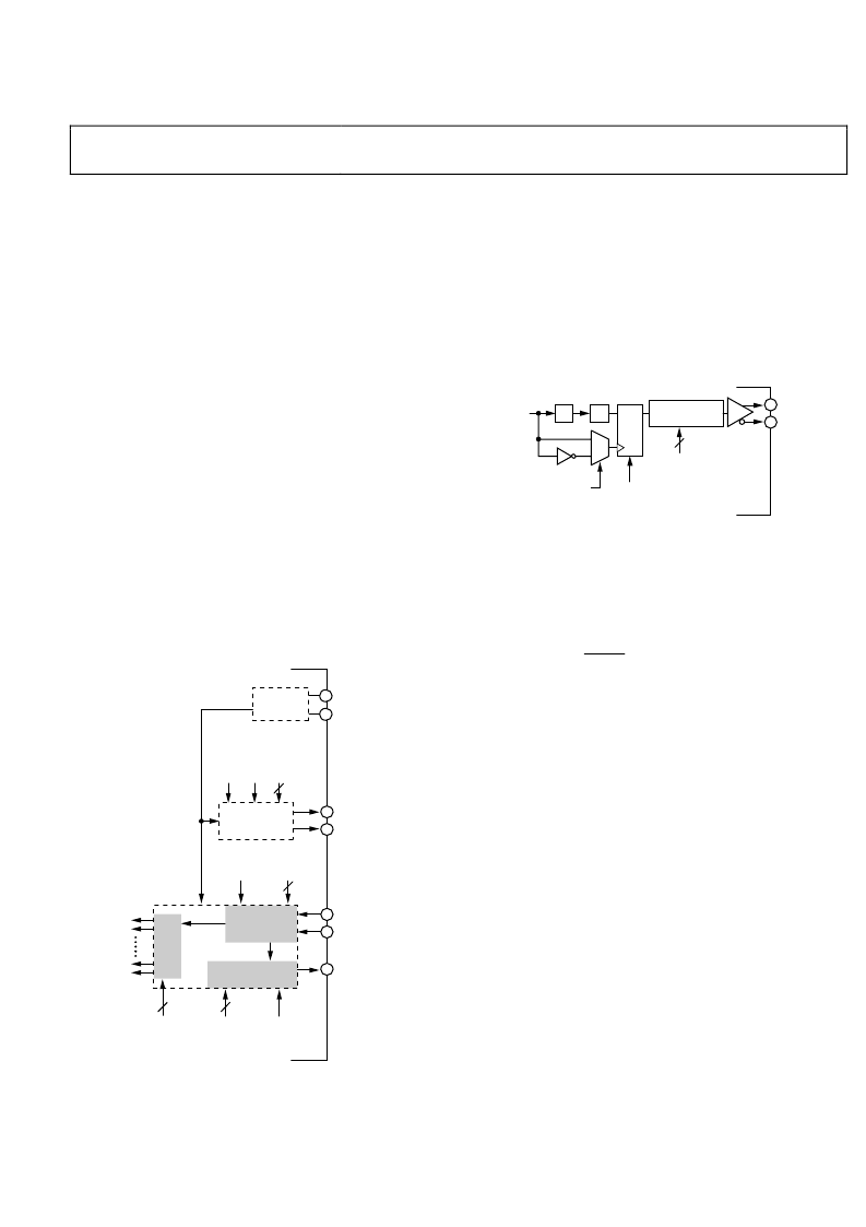
Figure 49. Synchronization Circuit Block Diagram
The synchronization mechanism relies on the premise that the
REFCLK signal appearing at each device is edge aligned with all
others as a result of the external REFCLK distribution system
(see Figure 52).
The sync generator block is shown in Figure 50. It is activated
via the sync generator enable bit. It allows for one AD9910 in a
group to function as a master timing source with the remaining
devices slaved to the master.
SYSCLK
SYNC
GENERATOR
ENABLE
SYNC
GEDELAY
SYNC
POLARITY
SYNC_OUT
0
1
D Q
R
PROGAMMABLE
DELAY
÷16
÷N
5
9
10
LVDS
DRIVER
0
Figure 50. Sync Generator Diagram
The sync generator produces a clock signal that appears at the
SYNC_OUT pins. This clock is delivered by an LVDS driver
and exhibits a 50% duty cycle. The clock has a fixed frequency
given by
f
f
=
16
_
SYSCLK
OUT
SYNC
The clock at the SYNC_OUT pins synchronizes with either the
rising or falling edge of the internal SYSCLK signal as deter-
mined by the sync generator polarity bit. Because the SYNC_OUT
signal is synchronized with the internal SYSCLK of the master
device, the master device SYSCLK serves as the reference timing
source for all slave devices. The user can adjust the output delay
of the SYNC_OUT signal in steps of ~150 ps by programming
the 5-bit sync generator delay word via the serial I/O port. The
programmable output delay facilitates added edge timing
flexibility to the overall synchronization mechanism.
The sync receiver block (shown in Figure 51) is activated via the
sync receiver enable bit. The sync receiver consists of three sub-
sections; the input delay and edge detection block, the internal
clock generator block, and the setup and hold validation block.
The clock generator block remains operational even if the sync
receiver is not enabled.
相關PDF資料 |
PDF描述 |
|---|---|
| AD9910BSVZ | 1 GSPS, 14-Bit, 3.3 V CMOS Direct Digital Synthesizer |
| AD9910BSVZ-REEL | 1 GSPS, 14-Bit, 3.3 V CMOS Direct Digital Synthesizer |
| AD9912 | 1 GSPS Direct Digital Synthesizer w/ 14-bit DAC |
| AD9913 | Low Power 250 MSPS 10-Bit DAC 1.8 V CMOS Direct Digital Synthesizer |
| AD9913BCPZ1 | Low Power 250 MSPS 10-Bit DAC 1.8 V CMOS Direct Digital Synthesizer |
相關代理商/技術參數 |
參數描述 |
|---|---|
| AD9910BSVZ | 功能描述:IC DDS 1GSPS 14BIT PAR 100TQFP RoHS:是 類別:集成電路 (IC) >> 接口 - 直接數字合成 (DDS) 系列:- 產品變化通告:Product Discontinuance 27/Oct/2011 標準包裝:2,500 系列:- 分辨率(位):10 b 主 fclk:25MHz 調節字寬(位):32 b 電源電壓:2.97 V ~ 5.5 V 工作溫度:-40°C ~ 85°C 安裝類型:表面貼裝 封裝/外殼:16-TSSOP(0.173",4.40mm 寬) 供應商設備封裝:16-TSSOP 包裝:帶卷 (TR) |
| AD9910BSVZ | 制造商:Analog Devices 功能描述:IC DDS 1GHZ TQFP-100 制造商:Analog Devices 功能描述:IC, DDS, 1GHZ, TQFP-100 |
| AD9910BSVZ-REEL | 功能描述:IC DDS 1GSPS 14BIT PAR 100TQFP RoHS:是 類別:集成電路 (IC) >> 接口 - 直接數字合成 (DDS) 系列:- 產品變化通告:Product Discontinuance 27/Oct/2011 標準包裝:2,500 系列:- 分辨率(位):10 b 主 fclk:25MHz 調節字寬(位):32 b 電源電壓:2.97 V ~ 5.5 V 工作溫度:-40°C ~ 85°C 安裝類型:表面貼裝 封裝/外殼:16-TSSOP(0.173",4.40mm 寬) 供應商設備封裝:16-TSSOP 包裝:帶卷 (TR) |
| AD9911 | 制造商:AD 制造商全稱:Analog Devices 功能描述:500 MSPS Direct Digital Synthesizer with 10-Bit DAC |
| AD9911/PCB | 制造商:Analog Devices 功能描述:500 MSPS DIRECT DGTL SYNTHESIZER W/ 10-BIT DAC AD9911/PCB - Bulk |
發布緊急采購,3分鐘左右您將得到回復。