- 您現在的位置:買賣IC網 > PDF目錄373970 > AD9910_07 (Analog Devices, Inc.) 1 GSPS, 14-Bit, 3.3 V CMOS Direct Digital Synthesizer PDF資料下載
參數資料
| 型號: | AD9910_07 |
| 廠商: | Analog Devices, Inc. |
| 元件分類: | XO, clock |
| 英文描述: | 1 GSPS, 14-Bit, 3.3 V CMOS Direct Digital Synthesizer |
| 中文描述: | 1 GSPS的,14位,3.3伏的CMOS直接數字頻率合成 |
| 文件頁數: | 47/60頁 |
| 文件大小: | 764K |
| 代理商: | AD9910_07 |
第1頁第2頁第3頁第4頁第5頁第6頁第7頁第8頁第9頁第10頁第11頁第12頁第13頁第14頁第15頁第16頁第17頁第18頁第19頁第20頁第21頁第22頁第23頁第24頁第25頁第26頁第27頁第28頁第29頁第30頁第31頁第32頁第33頁第34頁第35頁第36頁第37頁第38頁第39頁第40頁第41頁第42頁第43頁第44頁第45頁第46頁當前第47頁第48頁第49頁第50頁第51頁第52頁第53頁第54頁第55頁第56頁第57頁第58頁第59頁第60頁
AD9910
communication cycle can begin, starting with the instruction
byte write.
Rev. 0 | Page 47 of 60
I/O_UPDATE—Input/Output Update
The I/O_UPDATE initiates the transfer of written data from
the I/O port buffer to active registers. I/O_UPDATE is active
on the rising edge and its pulse width must be greater than one
SYNC_CLK period. It is either an input or output pin depending
on the programming of the Internal I/O update active bit.
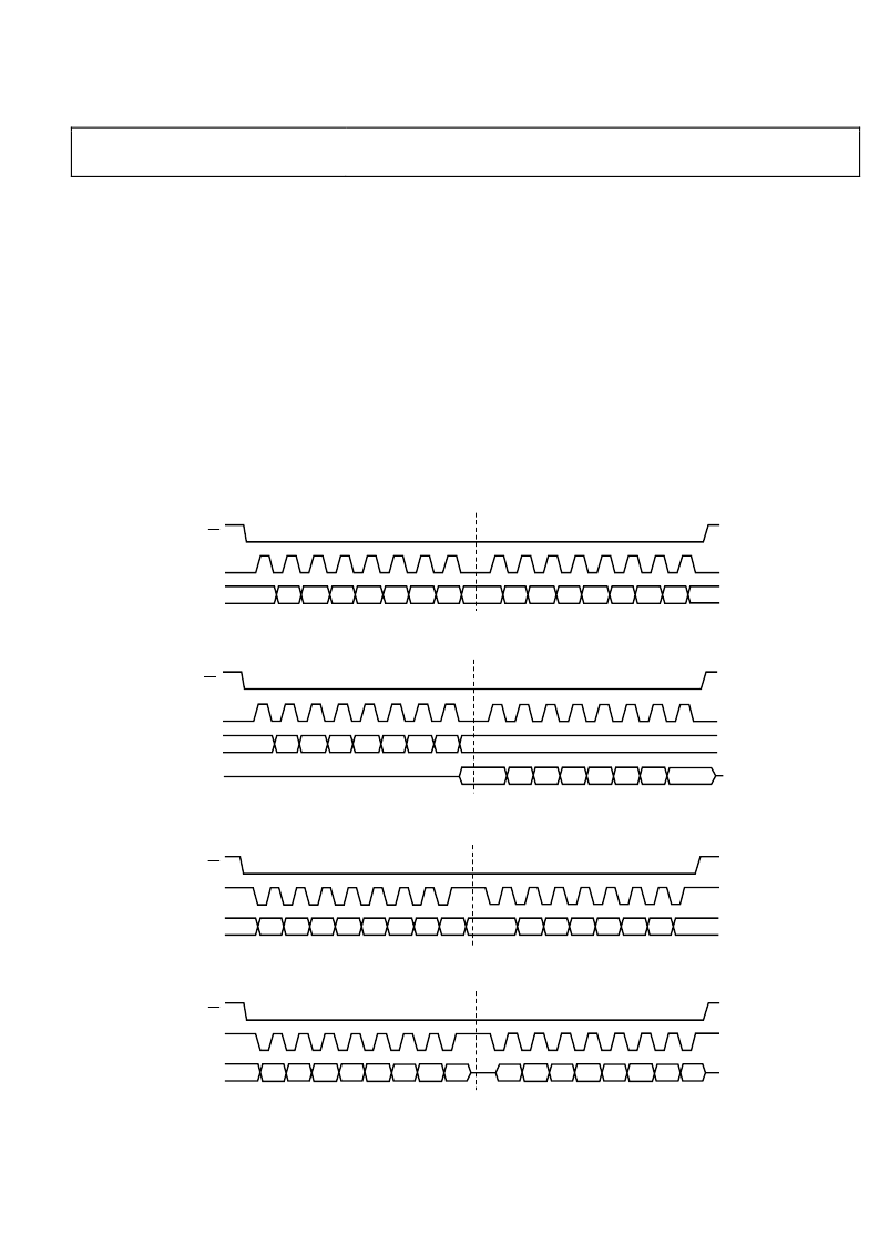
SERIAL I/O TIMING DIAGRAMS
The diagrams below provide basic examples of the timing
relationships between the various control signals of the serial
I/O port. Most of the bits in the register map are not transferred
to their internal destinations until assertion of an I/O update,
which is not included in the timing diagrams that follow.
MSB/LSB TRANSFERS
The AD9910 serial port can support both most significant bit
(MSB) first or least significant bit (LSB) first data formats. This
functionality is controlled by Bit 0 in Control Function
Register 1 (0x00). The default format is MSB first. If Bit 0 is set
high, the serial port is configured for LSB-first format. If LSB
first is active, all data, including the instruction byte, must
follow LSB-first convention. Note that the highest number
found in the bit range column for each register (see the Register
Map and Bit Descriptions section and Table 16) is the MSB and
the lowest number is the LSB for that register.
I
7
SDIO
INSTRUCTION CYCLE
DATA TRANSFER CYCLE
SCLK
CS
I
6
I
5
I
4
I
3
I
2
I
1
I
0
D
7
D
6
D
5
D
4
D
3
D
2
D
1
D
0
0
Figure 54. Serial Port Write Timing, Clock Stall Low
D
O7
INSTRUCTION CYCLE
DATA TRANSFER CYCLE
DON'T CARE
I
7
I
6
I
5
I
4
I
3
I
2
I
1
I
0
SDIO
SCLK
CS
SDO
D
O6
D
O5
D
O4
D
O3
D
O2
D
O1
D
O0
0
Figure 55. 3-Wire Serial Port Read Timing, Clock Stall Low
I
7
SDIO
INSTRUCTION CYCLE
DATA TRANSFER CYCLE
SCLK
CS
I
6
I
5
I
4
I
3
I
2
I
1
I
0
D
7
D
6
D
5
D
4
D
3
D
2
D
1
D
0
0
Figure 56. Serial Port Write Timing, Clock Stall High
I
7
SDIO
INSTRUCTION CYCLE
DATA TRANSFER CYCLE
SCLK
CS
I
6
I
5
I
4
I
3
I
2
I
1
I
0
D
O7
D
O6
D
O5
D
O4
D
O3
D
O2
D
O1
D
O0
0
Figure 57. 2-Wire Serial Port Read Timing, Clock Stall High
相關PDF資料 |
PDF描述 |
|---|---|
| AD9910BSVZ | 1 GSPS, 14-Bit, 3.3 V CMOS Direct Digital Synthesizer |
| AD9910BSVZ-REEL | 1 GSPS, 14-Bit, 3.3 V CMOS Direct Digital Synthesizer |
| AD9912 | 1 GSPS Direct Digital Synthesizer w/ 14-bit DAC |
| AD9913 | Low Power 250 MSPS 10-Bit DAC 1.8 V CMOS Direct Digital Synthesizer |
| AD9913BCPZ1 | Low Power 250 MSPS 10-Bit DAC 1.8 V CMOS Direct Digital Synthesizer |
相關代理商/技術參數 |
參數描述 |
|---|---|
| AD9910BSVZ | 功能描述:IC DDS 1GSPS 14BIT PAR 100TQFP RoHS:是 類別:集成電路 (IC) >> 接口 - 直接數字合成 (DDS) 系列:- 產品變化通告:Product Discontinuance 27/Oct/2011 標準包裝:2,500 系列:- 分辨率(位):10 b 主 fclk:25MHz 調節字寬(位):32 b 電源電壓:2.97 V ~ 5.5 V 工作溫度:-40°C ~ 85°C 安裝類型:表面貼裝 封裝/外殼:16-TSSOP(0.173",4.40mm 寬) 供應商設備封裝:16-TSSOP 包裝:帶卷 (TR) |
| AD9910BSVZ | 制造商:Analog Devices 功能描述:IC DDS 1GHZ TQFP-100 制造商:Analog Devices 功能描述:IC, DDS, 1GHZ, TQFP-100 |
| AD9910BSVZ-REEL | 功能描述:IC DDS 1GSPS 14BIT PAR 100TQFP RoHS:是 類別:集成電路 (IC) >> 接口 - 直接數字合成 (DDS) 系列:- 產品變化通告:Product Discontinuance 27/Oct/2011 標準包裝:2,500 系列:- 分辨率(位):10 b 主 fclk:25MHz 調節字寬(位):32 b 電源電壓:2.97 V ~ 5.5 V 工作溫度:-40°C ~ 85°C 安裝類型:表面貼裝 封裝/外殼:16-TSSOP(0.173",4.40mm 寬) 供應商設備封裝:16-TSSOP 包裝:帶卷 (TR) |
| AD9911 | 制造商:AD 制造商全稱:Analog Devices 功能描述:500 MSPS Direct Digital Synthesizer with 10-Bit DAC |
| AD9911/PCB | 制造商:Analog Devices 功能描述:500 MSPS DIRECT DGTL SYNTHESIZER W/ 10-BIT DAC AD9911/PCB - Bulk |
發布緊急采購,3分鐘左右您將得到回復。