- 您現在的位置:買賣IC網 > PDF目錄373970 > AD9910BSVZ (ANALOG DEVICES INC) 1 GSPS, 14-Bit, 3.3 V CMOS Direct Digital Synthesizer PDF資料下載
參數資料
| 型號: | AD9910BSVZ |
| 廠商: | ANALOG DEVICES INC |
| 元件分類: | DAC |
| 英文描述: | 1 GSPS, 14-Bit, 3.3 V CMOS Direct Digital Synthesizer |
| 中文描述: | SERIAL, PARALLEL, WORD INPUT LOADING, 14-BIT DAC, PDSO100 |
| 封裝: | ROHS COMPLIANT, MS-026AED-HD, TQFP-100 |
| 文件頁數: | 31/60頁 |
| 文件大小: | 764K |
| 代理商: | AD9910BSVZ |
第1頁第2頁第3頁第4頁第5頁第6頁第7頁第8頁第9頁第10頁第11頁第12頁第13頁第14頁第15頁第16頁第17頁第18頁第19頁第20頁第21頁第22頁第23頁第24頁第25頁第26頁第27頁第28頁第29頁第30頁當前第31頁第32頁第33頁第34頁第35頁第36頁第37頁第38頁第39頁第40頁第41頁第42頁第43頁第44頁第45頁第46頁第47頁第48頁第49頁第50頁第51頁第52頁第53頁第54頁第55頁第56頁第57頁第58頁第59頁第60頁
AD9910
No-Dwell Ramp Generation
The two no-dwell bits in Control Function Register 2 add to the
flexibility of the DRG capabilities. During normal ramp generation,
when the DRG output reaches the programmed upper or lower
limit, it simply remains at the limit until the operating parameters
dictate otherwise. However, during no-dwell operation, the DRG
output does not necessarily remain at the limit. For example, if the
digital ramp no-dwell high bit is set, when the DRG reaches the
upper limit it automatically (and immediately) snaps to the lower
limit (that is, it does not ramp back to the lower limit, it jumps to
the lower limit). Likewise, when the digital ramp no-dwell low bit
is set, when the DRG reaches the lower limit it automatically (and
immediately) snaps to the upper limit.
Rev. 0 | Page 31 of 60
During no-dwell operation, the DRCTL pin is monitored for state
transitions only, that is, the static logic level is immaterial.
During no-dwell high operation, a positive transition of the
DRCTL pin initiates a positive slope ramp, which continues
uninterrupted (regardless of any further activity on the DRCTL
pin) until the upper limit is reached.
During no-dwell low operation, a negative transition of the DRCTL
pin initiates a negative slope ramp, which continues uninterrupted
(regardless of any further activity on the DRCTL pin) until the
lower limit is reached.
Setting both no-dwell bits invokes a continuous ramping mode
of operation. That is, the DRG output automatically oscillates
between the two limits using the programmed slope parameters.
Furthermore, the function of the DRCTL pin is slightly different.
Instead of controlling the initiation of the ramp sequence, it
only serves to change the direction of the ramp. That is, if the
DRG output is in the midst of a positive slope and DRCTL pin
transitions from Logic 1 to Logic 0, then the DRG immediately
switches to the negative slope parameters and resumes oscilla-
tion between the limits. Likewise, if the DRG output is in the
midst of a negative slope and the DRCTL pin transitions from
Logic 0 to Logic 1, the DRG immediately switches to the positive
slope parameters and resumes oscillation between the limits.
When both no-dwell bits are set, the DROVER signal produces a
positive pulse (two cycles of the DDS clock) each time the DRG
output reaches either of the programmed limits (assuming that the
DROVER pin active bit is set).
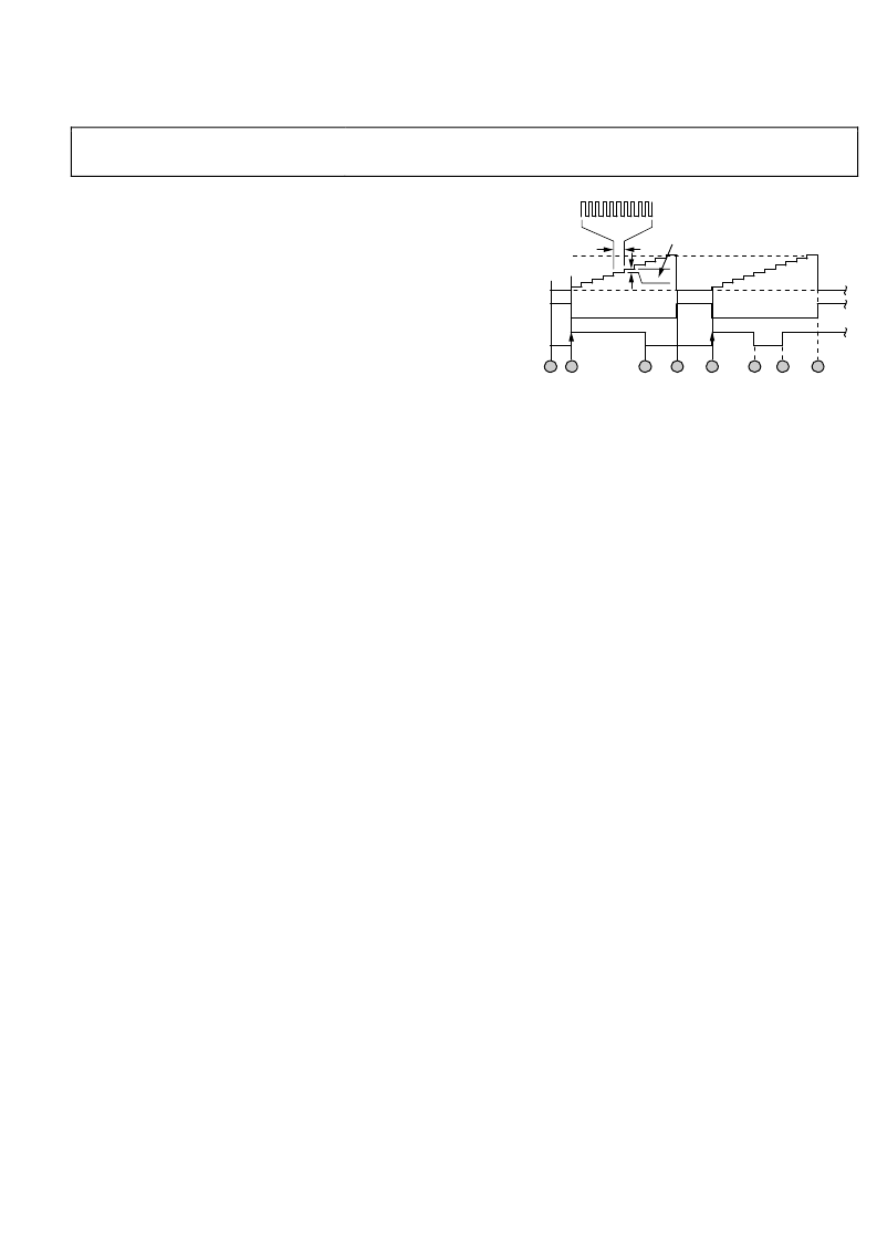
A no-dwell high DRG output waveform is shown in Figure 40.
The waveform diagram assumes that the digital ramp no-dwell
high bit is set and has been registered by an I/O update. The
status of the DROVER pin is also shown with the assumption
that the DROVER pin active bit has been set.
UPPER LIMIT
P DDS CLOCK CYCLES
1
2
3
4
5
6
7
8
DRG OUTPUT
LOWER LIMIT
DRCTL
POSITIVE
DROVER
+
Δ
t
0
Figure 40. No-Dwell High Ramp Generation
The circled numbers indicate specific events, which are explained
as follows:
Event 1—Indicates the instant that an I/O update registers that the
digital ramp enable bit has been set.
Event 2—DRCTL transitions to a Logic 1, initiating a positive
slope at the DRG output.
Event 3—DRCTL transition to a Logic 0, which has no effect on
the DRG output.
Event 4—Because the digital ramp no-dwell high bit is set, the
moment that the DRG output reaches the upper limit it immedi-
ately switches to the lower limit, where it remains until the next
Logic 0 to Logic 1 transition of DRCTL.
Event 5—DRCTL transitions from Logic 0 to Logic 1, which
restarts at positive slope ramp.
Event 6 and Event 7—DRCTL transitions are ignored until the
DRG output reaches the programmed upper limit.
Event 8—Because the digital ramp no-dwell high bit is set, the
moment that the DRG output reaches the upper limit it
immediately switches to the lower limit, where it remains until
the next Logic 0 to Logic 1 transition of DRCTL.
Operation with the digital ramp no-dwell low bit set (instead of the
digital ramp no-dwell high bit) is similar, except that the DRG
output ramps in the negative direction on a Logic 1 to Logic 0
transition of DRCTL and jumps to the upper limit upon reaching
the lower limit.
DROVER Pin
The DROVER pin provides an external signal to indicate the status
of the DRG. The functionality of this pin is controlled by the
DROVER pin active bit. When this bit is cleared (default), the
DROVER pin is always Logic 0 regardless of the status of the DRG.
When this bit is set, the DROVER pin logic level depends on the
status of the DRG. Specifically, when the DRG output is at either of
the programmed limits, the DROVER pin is Logic 1, otherwise, it is
Logic 0. In the special case of both no-dwell bits set, the DROVER
pin pulses positive for two DDS clock cycles each time the DRG
output reaches either of the programmed limits.
相關PDF資料 |
PDF描述 |
|---|---|
| AD9910BSVZ-REEL | 1 GSPS, 14-Bit, 3.3 V CMOS Direct Digital Synthesizer |
| AD9912 | 1 GSPS Direct Digital Synthesizer w/ 14-bit DAC |
| AD9913 | Low Power 250 MSPS 10-Bit DAC 1.8 V CMOS Direct Digital Synthesizer |
| AD9913BCPZ1 | Low Power 250 MSPS 10-Bit DAC 1.8 V CMOS Direct Digital Synthesizer |
| AD9913BCPZ-REEL71 | Low Power 250 MSPS 10-Bit DAC 1.8 V CMOS Direct Digital Synthesizer |
相關代理商/技術參數 |
參數描述 |
|---|---|
| AD9910BSVZ | 制造商:Analog Devices 功能描述:IC DDS 1GHZ TQFP-100 制造商:Analog Devices 功能描述:IC, DDS, 1GHZ, TQFP-100 |
| AD9910BSVZ-REEL | 功能描述:IC DDS 1GSPS 14BIT PAR 100TQFP RoHS:是 類別:集成電路 (IC) >> 接口 - 直接數字合成 (DDS) 系列:- 產品變化通告:Product Discontinuance 27/Oct/2011 標準包裝:2,500 系列:- 分辨率(位):10 b 主 fclk:25MHz 調節字寬(位):32 b 電源電壓:2.97 V ~ 5.5 V 工作溫度:-40°C ~ 85°C 安裝類型:表面貼裝 封裝/外殼:16-TSSOP(0.173",4.40mm 寬) 供應商設備封裝:16-TSSOP 包裝:帶卷 (TR) |
| AD9911 | 制造商:AD 制造商全稱:Analog Devices 功能描述:500 MSPS Direct Digital Synthesizer with 10-Bit DAC |
| AD9911/PCB | 制造商:Analog Devices 功能描述:500 MSPS DIRECT DGTL SYNTHESIZER W/ 10-BIT DAC AD9911/PCB - Bulk |
| AD9911/PCBZ | 功能描述:BOARD EVAL FOR AD9911 RoHS:是 類別:編程器,開發系統 >> 評估演示板和套件 系列:AgileRF™ 標準包裝:1 系列:PCI Express® (PCIe) 主要目的:接口,收發器,PCI Express 嵌入式:- 已用 IC / 零件:DS80PCI800 主要屬性:- 次要屬性:- 已供物品:板 |
發布緊急采購,3分鐘左右您將得到回復。