- 您現在的位置:買賣IC網 > PDF目錄373970 > AD9910BSVZ (ANALOG DEVICES INC) 1 GSPS, 14-Bit, 3.3 V CMOS Direct Digital Synthesizer PDF資料下載
參數資料
| 型號: | AD9910BSVZ |
| 廠商: | ANALOG DEVICES INC |
| 元件分類: | DAC |
| 英文描述: | 1 GSPS, 14-Bit, 3.3 V CMOS Direct Digital Synthesizer |
| 中文描述: | SERIAL, PARALLEL, WORD INPUT LOADING, 14-BIT DAC, PDSO100 |
| 封裝: | ROHS COMPLIANT, MS-026AED-HD, TQFP-100 |
| 文件頁數: | 32/60頁 |
| 文件大小: | 764K |
| 代理商: | AD9910BSVZ |
第1頁第2頁第3頁第4頁第5頁第6頁第7頁第8頁第9頁第10頁第11頁第12頁第13頁第14頁第15頁第16頁第17頁第18頁第19頁第20頁第21頁第22頁第23頁第24頁第25頁第26頁第27頁第28頁第29頁第30頁第31頁當前第32頁第33頁第34頁第35頁第36頁第37頁第38頁第39頁第40頁第41頁第42頁第43頁第44頁第45頁第46頁第47頁第48頁第49頁第50頁第51頁第52頁第53頁第54頁第55頁第56頁第57頁第58頁第59頁第60頁
AD9910
RAM CONTROL
RAM Overview
The AD9910 makes use of a 1024 × 32-bit RAM. The RAM has
two fundamental modes of operation: data entry/retrieve mode
and playback mode. Data entry/retrieve mode is active when
the RAM data is being loaded or read back via the serial I/O
port. Playback mode is active when the RAM contents are
routed to one of the internal data destinations.
Rev. 0 | Page 32 of 60
Depending on the specific playback mode, the user can
partition the RAM with up to eight independent time domain
waveforms. These waveforms drive the DDS signal control
parameters allowing for frequency, phase, amplitude, or polar
modulated signals.
RAM operations are enabled by setting the RAM enable bit in
Control Function Register 1; an I/O update (or a profile change)
is necessary to enact any change to the state of this bit.
Waveforms are generated using eight RAM profile registers that
are accessed via the three profile pins. Each profile contains the
following:
10-bit waveform start address word
10-bit waveform end address word
16-bit address step rate control word
3-bit RAM mode control word
No-dwell high bit
Zero-crossing bit
The user must ensure that the end address is greater than the
start address.
Each profile defines the number of samples and the sample rate
for a given waveform. In conjunction with an internal state
machine, the RAM contents are delivered to the appropriate
DDS signal control parameter(s) at the specified rate. Further-
more, the state machine can control the order in which samples
are extracted from RAM (forward/reverse), facilitating efficient
generation of time symmetric waveforms.
Load/Retrieve RAM Operation
It is strongly recommended that RAM enable = 0 when
performing RAM load/retrieve operations. Loading or
retrieving the contents of the RAM requires a three-step
process.
1.
Program the RAM Profile<0:7> registers with the start and
end addresses that are to define the boundaries of each
independent waveform.
Drive the appropriate logic levels on the profile pins to
select the desired RAM profile.
2.
3.
Write (or read) the address range specified by the selected
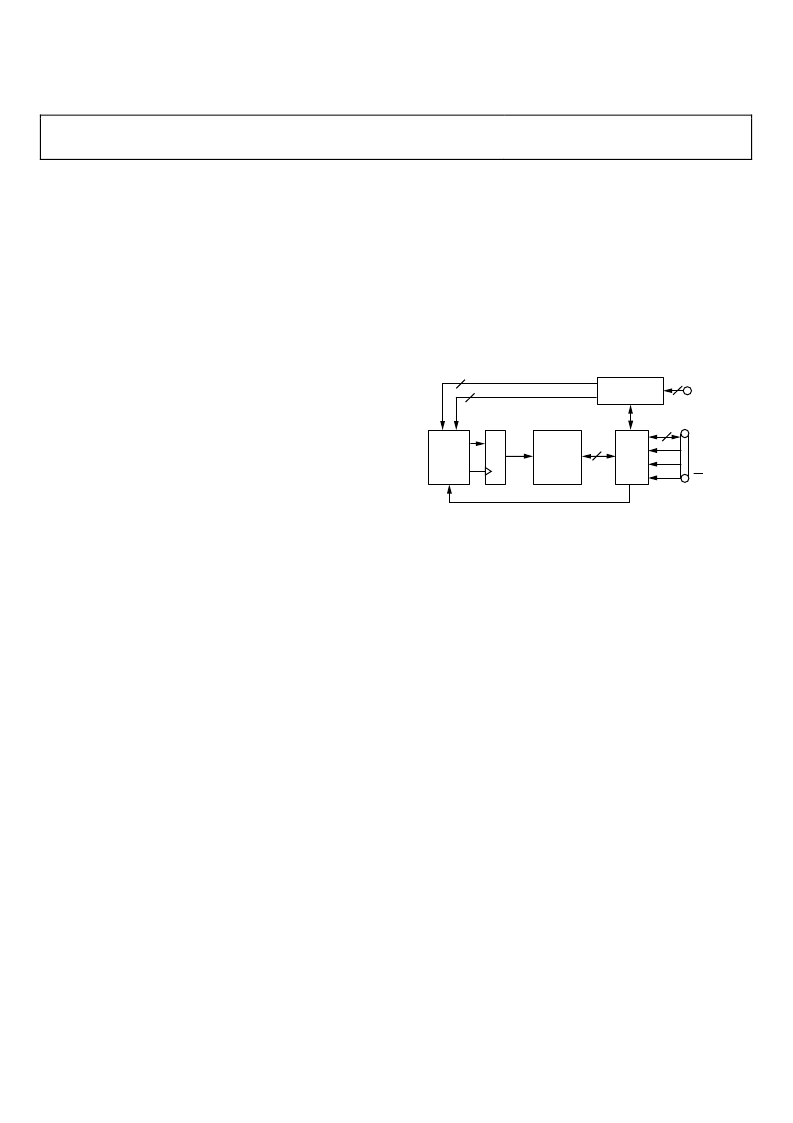
RAM profile via the serial port (see the Serial Programming
section for details). Figure 41 is a block diagram showing
the functional components used for RAM data load/retrieve
operation.
During RAM load/retrieve operations, the state machine controls
an up/down counter to step through the required RAM loca-
tions. The counter synchronizes with the serial I/O port so that
the serial/parallel conversion of the 32-bit words is correctly
timed with the generation of the appropriate RAM address to
properly execute the desired read or write operation.
RAM
A
D
Q
SCLK
I/O_RESET
SDIO
CS
PROFILE
WAVEFORM END ADDRESS
WAVEFORM START ADDRESS
ADDRESS CLOCK
PROGRAMMING
REGISTERS
STATE
MACHINE
UP/DOWN
COUNTER
SERIAL
I/O
PORT
2
32
10
10
U/D
3
0
Figure 41. RAM Data Load/Retrieve Operation
The RAM profiles are completely independent; it is possible
to define overlapping address ranges. Doing so causes data
that has been written to overlapped address locations to be
overwritten by the most recent write operation.
Multiple waveforms can be loaded into RAM by treating them
as a single waveform, that is, a time-domain concatenation of all
the waveforms. This is done by programming one of the RAM
profiles with a start and end address spanning the entire range
of the concatenated waveforms. Then the single concatenated
waveform is written into RAM via the serial I/O port using the
same RAM profile that was programmed with the start and end
addresses. The RAM profiles must then be programmed with
the proper start and end addresses associated with each
individual
waveform
.
RAM Playback Operation (Waveform Generation)
When the RAM has been loaded with the desired waveform
data, it can then be used for waveform generation during
playback. RAM playback requires that RAM enable = 1. To
playback RAM data select the desired waveform using the
profile pins. The selected profile directs the internal state
machine by defining the RAM address range occupied by the
waveform, the rate at which samples are to be extracted from
the RAM (playback rate), the mode of operation, and whether
to use the no-dwell feature. Figure 42 is a block diagram
showing the functional components used for RAM playback
operation.
相關PDF資料 |
PDF描述 |
|---|---|
| AD9910BSVZ-REEL | 1 GSPS, 14-Bit, 3.3 V CMOS Direct Digital Synthesizer |
| AD9912 | 1 GSPS Direct Digital Synthesizer w/ 14-bit DAC |
| AD9913 | Low Power 250 MSPS 10-Bit DAC 1.8 V CMOS Direct Digital Synthesizer |
| AD9913BCPZ1 | Low Power 250 MSPS 10-Bit DAC 1.8 V CMOS Direct Digital Synthesizer |
| AD9913BCPZ-REEL71 | Low Power 250 MSPS 10-Bit DAC 1.8 V CMOS Direct Digital Synthesizer |
相關代理商/技術參數 |
參數描述 |
|---|---|
| AD9910BSVZ | 制造商:Analog Devices 功能描述:IC DDS 1GHZ TQFP-100 制造商:Analog Devices 功能描述:IC, DDS, 1GHZ, TQFP-100 |
| AD9910BSVZ-REEL | 功能描述:IC DDS 1GSPS 14BIT PAR 100TQFP RoHS:是 類別:集成電路 (IC) >> 接口 - 直接數字合成 (DDS) 系列:- 產品變化通告:Product Discontinuance 27/Oct/2011 標準包裝:2,500 系列:- 分辨率(位):10 b 主 fclk:25MHz 調節字寬(位):32 b 電源電壓:2.97 V ~ 5.5 V 工作溫度:-40°C ~ 85°C 安裝類型:表面貼裝 封裝/外殼:16-TSSOP(0.173",4.40mm 寬) 供應商設備封裝:16-TSSOP 包裝:帶卷 (TR) |
| AD9911 | 制造商:AD 制造商全稱:Analog Devices 功能描述:500 MSPS Direct Digital Synthesizer with 10-Bit DAC |
| AD9911/PCB | 制造商:Analog Devices 功能描述:500 MSPS DIRECT DGTL SYNTHESIZER W/ 10-BIT DAC AD9911/PCB - Bulk |
| AD9911/PCBZ | 功能描述:BOARD EVAL FOR AD9911 RoHS:是 類別:編程器,開發系統 >> 評估演示板和套件 系列:AgileRF™ 標準包裝:1 系列:PCI Express® (PCIe) 主要目的:接口,收發器,PCI Express 嵌入式:- 已用 IC / 零件:DS80PCI800 主要屬性:- 次要屬性:- 已供物品:板 |
發布緊急采購,3分鐘左右您將得到回復。