- 您現(xiàn)在的位置:買賣IC網 > PDF目錄373995 > ADM1060 (Analog Devices, Inc.) DIP Socket; No. of Contacts:56; Pitch Spacing:0.07"; Row Spacing:0.6"; Terminal Type:PC Board; Leaded Process Compatible:Yes; Peak Reflow Compatible (260 C):No RoHS Compliant: Yes PDF資料下載
參數(shù)資料
| 型號: | ADM1060 |
| 廠商: | Analog Devices, Inc. |
| 英文描述: | DIP Socket; No. of Contacts:56; Pitch Spacing:0.07"; Row Spacing:0.6"; Terminal Type:PC Board; Leaded Process Compatible:Yes; Peak Reflow Compatible (260 C):No RoHS Compliant: Yes |
| 中文描述: | 通信系統(tǒng)監(jiān)控/排序電路 |
| 文件頁數(shù): | 27/45頁 |
| 文件大小: | 303K |
| 代理商: | ADM1060 |
第1頁第2頁第3頁第4頁第5頁第6頁第7頁第8頁第9頁第10頁第11頁第12頁第13頁第14頁第15頁第16頁第17頁第18頁第19頁第20頁第21頁第22頁第23頁第24頁第25頁第26頁當前第27頁第28頁第29頁第30頁第31頁第32頁第33頁第34頁第35頁第36頁第37頁第38頁第39頁第40頁第41頁第42頁第43頁第44頁第45頁
ADM1060 LOGIC
ADM1060
–
27
–
REV. PrJ 11/02
PRELIMINARY TECHNICAL DATA
PROGRAMMABLE DE LAY BLOCK
Each output of the PLBA is fed into a separate Program-
mable Delay Block (PDB). T he PDB enables the user to
add a delay to the logic block output before it is applied to
either a PDO or one of the other PLB
’
s (the output of a
PLB can be the input to any of the other PLB
’
s- not it-
self). T he PDB operation is similar to that of the glitch
filter (discussed in the SFD section). T here is an impor-
tant difference between the 2 functions, however. T he
delay on the falling edge of an input to the PDB can be
programmed independently of the rising edge. T his al-
lows the user to program the length of the pulse outputted
from the PDB. T hus, for instance, the width of the pulse
from the Watchdog Fault Detector can be adjusted, or the
user can ensure that a supply supervised by one of the
SFD
’
s is within its UV/OV range for a programmed pe-
riod of time before asserting a PDO. A delay of between
0ms and 500ms can be programmed in the PnPDBT IM
registers. 4 bits each are used to program the rising edge
and falling edge. Once programmed, the PDB operates as
follows. If the user programs a delay on the rising edge
of, say, 200ms, the PDB looks for a rising edge on the
input. Once it sees the edge it starts a timer. If the input
remains high and the timer reaches 200ms, then the PDB
immediately outputs a rising edge. If the input falls low
before the timer has reached 200ms then no edge is out-
putted from the PDB and the timer is reset. Because there
is separate control over the falling edge, if no delay is
programmed on the falling edge, the delay defaults to 0
and a falling edge on the input will immediately appear on
the output. If a falling edge delay is programmed, then
the PDB operates exactly the opposite to the way it does
for a rising edge. Again, if a delay of, say, 200ms is pro-
grammed on the falling edge, the PDB looks for a falling
edge on the input. Once it sees the edge, it again starts a
timer. If the input remains low and the timer reaches
200ms, then the output transitions from high to low. A
valid rising edge must appear at the output before a falling
edge delay can be activated. T he function of the PDB is
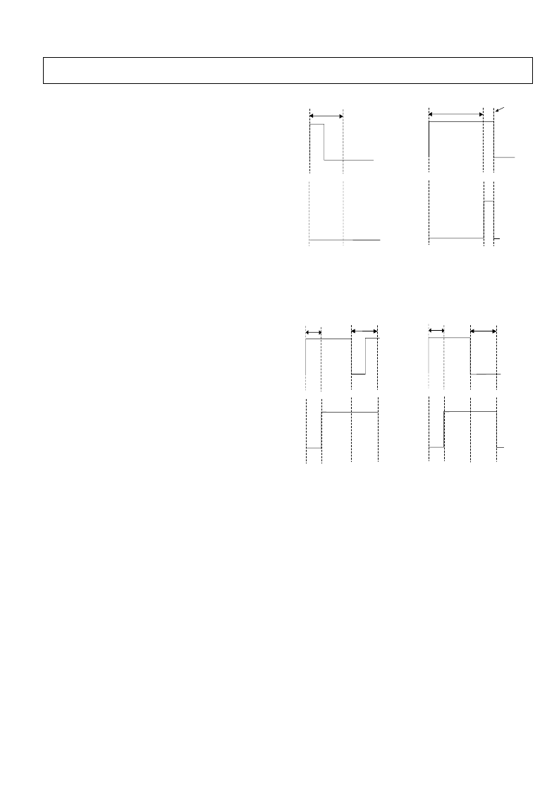
illustrated in figure 6 below.
Aside from the extra timing flexibility offered, the pro-
grammable delay also provides a crude form of filtering.
In much the same way as the Glitch Filter operates, an
input must be high (or low) for a programmed period of
time before being seen on the output. T ransients which
are shorter that the programmed timeouts will not appear
on the output. T he bitmap for the register which controls
both the rising and falling edges is shown overleaf:-
Figure 6. Functionality of the Programmable Delay Block (PDB)
#*#00$#+$'0$
#*#00$%'0$21
-)&'
-&'&'
#*#00$#+$'0$
#*#00$#+$'0$
#*#00$%'0$
'1
'#+$
'1
'#+$'%
'1
'#+$'%
'1
'#+$
'%
'
'1
'#+$
'%
'
#*#00$#+$'0$
#*#00$%'0$
'1
'#+$
'%
'
'1
'#+$
'%
'
'1
'#+$
#*#00)*#+$'0$)3
#*#00)*#+$'0$)%'0$
-&'&'
-)&'
相關PDF資料 |
PDF描述 |
|---|---|
| ADM1060ARU | CON-HDR64POS2ROW 4WALL.1X.1SP,RTANG,LOPF |
| ADM1064 | Super Sequencer with Voltage Readback ADC |
| ADM1064ACP | Super Sequencer with Voltage Readback ADC |
| ADM1064ACP-REEL | Super Sequencer with Voltage Readback ADC |
| ADM1064ACP-REEL7 | Super Sequencer with Voltage Readback ADC |
相關代理商/技術參數(shù) |
參數(shù)描述 |
|---|---|
| ADM1060ARU | 功能描述:IC SUPERVIS/SEQUENC 7-CH 28TSSOP RoHS:否 類別:集成電路 (IC) >> PMIC - 監(jiān)控器 系列:Super Sequencer® 標準包裝:1 系列:- 類型:簡單復位/加電復位 監(jiān)視電壓數(shù)目:1 輸出:開路漏極或開路集電極 復位:高有效 復位超時:- 電壓 - 閥值:1.8V 工作溫度:-40°C ~ 125°C 安裝類型:表面貼裝 封裝/外殼:6-TSOP(0.059",1.50mm 寬)5 引線 供應商設備封裝:5-TSOP 包裝:剪切帶 (CT) 其它名稱:NCP301HSN18T1GOSCT |
| ADM1060ARUCS0001R7 | 功能描述:IC SUPERVISOR/SEQUENCER 制造商:analog devices inc. 系列:* 零件狀態(tài):上次購買時間 標準包裝:1 |
| ADM1060ARUCS0100R7 | 功能描述:IC SUPERVISOR/SEQUENCER 制造商:analog devices inc. 系列:* 零件狀態(tài):上次購買時間 標準包裝:1 |
| ADM1060ARUCS0101R7 | 功能描述:IC SUPERVISOR/SEQUENCER 制造商:analog devices inc. 系列:* 零件狀態(tài):上次購買時間 標準包裝:1 |
| ADM1060ARUCS0102R7 | 功能描述:IC SUPERVISOR/SEQUENCER 制造商:analog devices inc. 系列:* 零件狀態(tài):上次購買時間 標準包裝:1 |
發(fā)布緊急采購,3分鐘左右您將得到回復。