- 您現在的位置:買賣IC網 > PDF目錄373995 > ADM1060ARU (ANALOG DEVICES INC) CON-HDR64POS2ROW 4WALL.1X.1SP,RTANG,LOPF PDF資料下載
參數資料
| 型號: | ADM1060ARU |
| 廠商: | ANALOG DEVICES INC |
| 元件分類: | 電源管理 |
| 英文描述: | CON-HDR64POS2ROW 4WALL.1X.1SP,RTANG,LOPF |
| 中文描述: | 7-CHANNEL POWER SUPPLY MANAGEMENT CKT, PDSO28 |
| 封裝: | MO-153AE, TSSOP-28 |
| 文件頁數: | 18/45頁 |
| 文件大小: | 303K |
| 代理商: | ADM1060ARU |
第1頁第2頁第3頁第4頁第5頁第6頁第7頁第8頁第9頁第10頁第11頁第12頁第13頁第14頁第15頁第16頁第17頁當前第18頁第19頁第20頁第21頁第22頁第23頁第24頁第25頁第26頁第27頁第28頁第29頁第30頁第31頁第32頁第33頁第34頁第35頁第36頁第37頁第38頁第39頁第40頁第41頁第42頁第43頁第44頁第45頁
ADM1060
ADM1060 LOGIC
–
18
–
REV. PrJ 11/02
PRELIMINARY TECHNICAL DATA
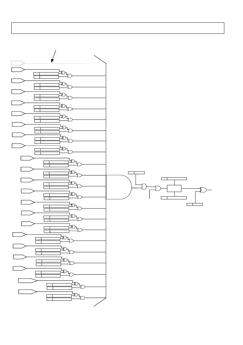
Figure 5. Detailed Diagram for function A of PLB1
T he diagram shown highlights all 21 inputs to a given
function and the register/ bits which need to be set in
order to condition the 21 inputs correctly. T he diagram
only shows function A of Programmable Logic Block 1
(PLB1) but all functions are programmed in the same way.
If, as an example, the user wishes to assert PLBOUT
200ms after all of the supplies are in spec. (PLBOUT may
be used to drive the enable pin of an LDO) then the
supply fault detectors VBn, VH and VPn are required to
control the function. T he function is programmed as
follows:-
T he IGNORE bit of all the other inputs (GPI
’
s, PDB
’
s
WDI) in the relevant P1xxxIMK registers is set to 1.
T hus, regardless of their status, the input to the function
AND gate for these inputs will be 1.
Since the SFD
’
s assert a 1 under a fault condition and a
0 when the supplies are in tolerance, the SFD outputs
need to be inverted before being applied to the function.
T hus the relevant bit in the P1SFDPOL register is set
(See T able Y).
T he function is enabled (bit 1 of register P1EN- T able
Z))
A rise time of 200ms is programmed (register
P1PDBT IM- see register map overleaf for details)
ENABLE
FUNCTION A
07H P1EN.1
PLB2
00H P1PLBPOLA.0
01H P1PLBIMKA.0
INVERT
IGNORE
TO
FUNCTION B
PDB
RISE TIME
0CH P1PDBTIM.7-4
FALL TIME
PLB3
00H P1PLBPOLA.1
01H P1PLBIMKA.1
INVERT
IGNORE
PLB4
00H P1PLBPOLA.2
01H P1PLBIMKA.2
INVERT
IGNORE
PLB5
00H P1PLBPOLA.3
01H P1PLBIMKA.3
INVERT
IGNORE
PLB6
00H P1PLBPOLA.4
01H P1PLBIMKA.4
INVERT
IGNORE
PLB7
00H P1PLBPOLA.5
01H P1PLBIMKA.5
INVERT
IGNORE
PLB8
00H P1PLBPOLA.6
01H P1PLBIMKA.6
INVERT
IGNORE
PLB9
00H P1PLBPOLA.7
01H P1PLBIMKA.7
INVERT
IGNORE
VB1
02H P1SFDPOLA.0
03H P1SFDIMKA.0
INVERT
IGNORE
VB2
02H P1SFDPOLA.1
03H P1SFDIMKA.1
INVERT
IGNORE
VH
02H P1SFDPOLA.2
03H P1SFDIMKA.2
INVERT
IGNORE
VP1
02H P1SFDPOLA.3
03H P1SFDIMKA.3
INVERT
IGNORE
VP2
02H P1SFDPOLA.4
03H P1SFDIMKA.4
INVERT
IGNORE
VP3
02H P1SFDPOLA.5
03H P1SFDIMKA.5
INVERT
IGNORE
VP4
02H P1SFDPOLA.6
03H P1SFDIMKA.6
INVERT
IGNORE
GPI1
04H P1GPIPOL.4
05H P1GPIIMK.4
INVERT
IGNORE
GPI2
04H P1GPIPOL.5
05H P1GPIIMK.5
INVERT
IGNORE
GPI3
04H P1GPIPOL.6
05H P1GPIIMK.6
INVERT
IGNORE
GPI4
04H P1GPIPOL.7
05H P1GPIIMK.7
INVERT
IGNORE
WDI_P
06H P1WDICFG.7
06H P1WDICFG.6
INVERT
IGNORE
WDI_L
06H P1WDICFG.5
06H P1WDICFG.4
INVERT
IGNORE
0CH P1PDBTIM.3-0
07H P1EN.2
PLBOUT
PLB1
(ie) Not Connected
相關PDF資料 |
PDF描述 |
|---|---|
| ADM1064 | Super Sequencer with Voltage Readback ADC |
| ADM1064ACP | Super Sequencer with Voltage Readback ADC |
| ADM1064ACP-REEL | Super Sequencer with Voltage Readback ADC |
| ADM1064ACP-REEL7 | Super Sequencer with Voltage Readback ADC |
| ADM1064ASU | Super Sequencer with Voltage Readback ADC |
相關代理商/技術參數 |
參數描述 |
|---|---|
| ADM1060ARUCS0001R7 | 功能描述:IC SUPERVISOR/SEQUENCER 制造商:analog devices inc. 系列:* 零件狀態:上次購買時間 標準包裝:1 |
| ADM1060ARUCS0100R7 | 功能描述:IC SUPERVISOR/SEQUENCER 制造商:analog devices inc. 系列:* 零件狀態:上次購買時間 標準包裝:1 |
| ADM1060ARUCS0101R7 | 功能描述:IC SUPERVISOR/SEQUENCER 制造商:analog devices inc. 系列:* 零件狀態:上次購買時間 標準包裝:1 |
| ADM1060ARUCS0102R7 | 功能描述:IC SUPERVISOR/SEQUENCER 制造商:analog devices inc. 系列:* 零件狀態:上次購買時間 標準包裝:1 |
| ADM1060ARUCS0103R7 | 制造商:Analog Devices 功能描述: |
發布緊急采購,3分鐘左右您將得到回復。