- 您現在的位置:買賣IC網 > PDF目錄374046 > ADV7180 (Analog Devices, Inc.) 10-Bit, 4 x Oversampling SDTV Video Decoder PDF資料下載
參數資料
| 型號: | ADV7180 |
| 廠商: | Analog Devices, Inc. |
| 英文描述: | 10-Bit, 4 x Oversampling SDTV Video Decoder |
| 中文描述: | 10位,4個采樣標清視頻解碼器 |
| 文件頁數: | 13/112頁 |
| 文件大小: | 1320K |
| 代理商: | ADV7180 |
第1頁第2頁第3頁第4頁第5頁第6頁第7頁第8頁第9頁第10頁第11頁第12頁當前第13頁第14頁第15頁第16頁第17頁第18頁第19頁第20頁第21頁第22頁第23頁第24頁第25頁第26頁第27頁第28頁第29頁第30頁第31頁第32頁第33頁第34頁第35頁第36頁第37頁第38頁第39頁第40頁第41頁第42頁第43頁第44頁第45頁第46頁第47頁第48頁第49頁第50頁第51頁第52頁第53頁第54頁第55頁第56頁第57頁第58頁第59頁第60頁第61頁第62頁第63頁第64頁第65頁第66頁第67頁第68頁第69頁第70頁第71頁第72頁第73頁第74頁第75頁第76頁第77頁第78頁第79頁第80頁第81頁第82頁第83頁第84頁第85頁第86頁第87頁第88頁第89頁第90頁第91頁第92頁第93頁第94頁第95頁第96頁第97頁第98頁第99頁第100頁第101頁第102頁第103頁第104頁第105頁第106頁第107頁第108頁第109頁第110頁第111頁第112頁
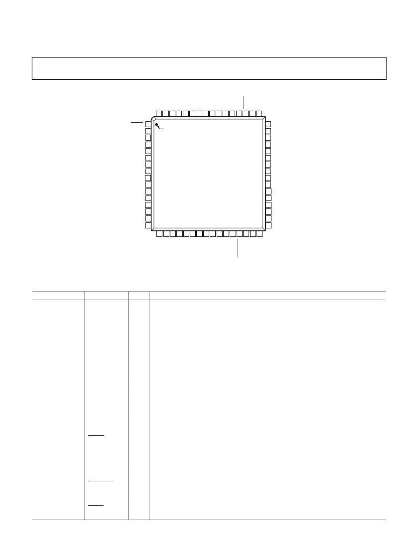
ADV7180
64-LEAD LQFP
Rev. A | Page 13 of 113
64
V
63
F
62
P
61
P
60
P
59
P
58
D
57
D
56
G
55
G
54
S
53
S
52
A
51
R
50
N
49
A
I
6
47
A
IN
4
46
A
IN
3
45
NC
42
NC
43
AGND
44
NC
48
A
IN
5
41
NC
40
AVDD
39
VREFN
37
AGND
36
A
IN
2
35
A
IN
1
34
TEST_0
33
NC
38
VREFP
2
HS
3
DGND
4
DVDDIO
7
P9
P8
6
P10
5
P11
1
INTRQ
8
9
SFL
10
DGND
12
GPO1
13
GPO0
14
P7
15
P6
16
P5
11
DVDDIO
17
P
18
P
19
P
20
L
21
X
22
X
23
D
24
D
25
P
26
P
27
N
28
N
29
P
30
E
31
P
32
A
PIN 1
ADV7180
LQFP
TOP VIEW
(Not to Scale)
NC = NO CONNECT
0
Figure 8. 64-Lead LQFP Pin Configuration
Table 9. Pin Function Description for the ADV7180 LQFP-64
Pin No.
Mnemonic
3, 10, 24, 57
DGND
32, 37, 43
AGND
4, 11
DVDDIO
23, 58
DVDD
40
AVDD
31
PVDD
38
VREFP
39
VREFN
35, 36, 46 to 49
A
IN
1 to A
IN
6
27, 28, 33, 41, 42,
44, 45, 50
5 to 8, 14 to 19,
25, 26, 59 to 62
P7 to P2, P1,
P0, P15 to P12
2
HS
64
VS
63
FIELD
1
INTRQ
Type
G
G
P
P
P
P
O
O
I
Function
Digital Ground.
Analog Ground.
Digital I/O Supply Voltage (3.3 V).
Digital Supply Voltage (1.8 V).
Analog Supply Voltage (1.8 V).
PLL Supply Voltage (1.8 V).
Internal Voltage Reference Output. See Figure 54 for recommended output circuitry.
Internal Voltage Reference Output. See Figure 54 for recommended output circuitry.
Analog Video Input Channels.
No Connect Pins. These pins are not connected internally.
NC
P11 to P8,
O
Video Pixel Output Port. See Table 96 for output configuration for 8-bit and 16-bit modes.
O
O
O
O
Horizontal Synchronization Output Signal.
Vertical Synchronization Output Signal.
Field Synchronization Output Signal.
Interrupt Request Output. Interrupt occurs when certain signals are detected on the input
video (see Table 104).
I
2
C Port Serial Data Input/Output Pin.
I
2
C Port Serial Clock Input. Maximum clock rate of 400 kHz.
This pin selects the I
2
C address for the ADV7180. For ALSB set to Logic 0, the address
selected for a write is 0x40; for ALSB set to logic high, the address selected is 0x42.
A logic low on this pin places the ADV7180 in power-down mode.
The recommended external loop filter must be connected to the ELPF pin, as shown in
Figure 54.
System Reset Input. Active low. A minimum low reset pulse width of 5 ms is required to reset
the ADV7180 circuitry.
53
54
52
SDATA
SCLK
ALSB
I/O
I
I
29
30
PWRDWN
ELPF
I
I
51
RESET
I
相關PDF資料 |
PDF描述 |
|---|---|
| ADV7180BCPZ | 10-Bit, 4 x Oversampling SDTV Video Decoder |
| ADV7180BSTZ | 10-Bit, 4 x Oversampling SDTV Video Decoder |
| ADV7181 | Multiformat SDTV Video Decoder |
| ADV7181B | Multiformat SDTV Video Decoder |
| ADV7181BBCPZ | Multiformat SDTV Video Decoder |
相關代理商/技術參數 |
參數描述 |
|---|---|
| ADV7180_12 | 制造商:AD 制造商全稱:Analog Devices 功能描述:10-Bit, 4?? Oversampling SDTV Video Decoder |
| ADV7180BCP32Z | 制造商:Analog Devices 功能描述:10-BIT, 4? OVERSAMPLING SDTV VIDEO DECODER - Trays |
| ADV7180BCP32Z-RL | 制造商:Analog Devices 功能描述:IC |
| ADV7180BCPZ | 功能描述:IC VIDEO DECODER SDTV 40-LFCSP RoHS:是 類別:集成電路 (IC) >> 線性 - 視頻處理 系列:- 標準包裝:250 系列:- 類型:電平移位器 應用:LCD 電視機/監控器 安裝類型:表面貼裝 封裝/外殼:28-WFQFN 裸露焊盤 供應商設備封裝:28-WQFN(4x4)裸露焊盤 包裝:帶卷 (TR) 其它名稱:296-32523-2TPS65198RUYT-ND |
| ADV7180BCPZ | 制造商:Analog Devices 功能描述:IC VIDEO DECODER 10BIT 57.27MSPS LFCSP40 |
發布緊急采購,3分鐘左右您將得到回復。