- 您現(xiàn)在的位置:買賣IC網(wǎng) > PDF目錄365968 > TSB14AA1I FPGA (Field-Programmable Gate Array) PDF資料下載
參數(shù)資料
| 型號(hào): | TSB14AA1I |
| 英文描述: | FPGA (Field-Programmable Gate Array) |
| 中文描述: | 電信提供商/數(shù)據(jù)通信 |
| 文件頁數(shù): | 10/35頁 |
| 文件大小: | 224K |
| 代理商: | TSB14AA1I |
第1頁第2頁第3頁第4頁第5頁第6頁第7頁第8頁第9頁當(dāng)前第10頁第11頁第12頁第13頁第14頁第15頁第16頁第17頁第18頁第19頁第20頁第21頁第22頁第23頁第24頁第25頁第26頁第27頁第28頁第29頁第30頁第31頁第32頁第33頁第34頁第35頁
1
–
5
1.5
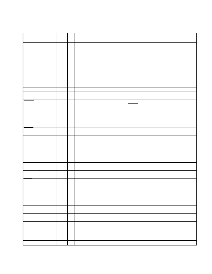
Terminal Descriptions (Continued)
TERMINAL
TYPE
I/O
DESCRIPTION
NAME
LPS
NO.
1
CMOS
I
Link power status input. This pin monitors the active/power status of the link layer controller and
controls the state of the PHY-LLC interface. This pin must be connected to either a pulsed output that
is active when the LLC is powered, or to the VDD supplying the LLC through a 10-k
resistor. The LPS
input is considered inactive if it is sampled low by the PHY for more than 128 SCLK cycles and is
considered active otherwise (i.e., asserted steady high or an oscillating signal with a low time less
than 2.6
μ
s). The LPS input must be high for at least 21 ns in order to ensure observation as high by
the PHY.
When the TSB14AA1A detects that LPS is inactive, it will place the PHY-LLC interface into a
low
–
power reset state. In the reset state, the CTL and D outputs are held in the logic zero state and
the LREQ input is ignored; however, the SCLK output remains active. If the LPS input remains low for
more than 1280 SCLK cycles, the PHY-LLC interface is placed into a low-power disabled state in
which the SCLK output is also held inactive. The PHY-LLC interface is placed into the disabled state
upon hardware reset. The LLC is considered active only if the LPS input is active.
Link request input. The LLC uses this input to initiate a service request to the TSB14AA1A.
LREQ
3
CMOS
I
M-TEST
26
CMOS
I
Manufacturing tests. When M-TEST is set high, manufacturing test modes are enabled. For normal
operation, this pin must be set low.
OCDOE
25
CMOS
O
Open collector driver output enable pin. This pin is driven low to enable the open-collector
transceivers for both TDATA and TSTRB. OCDOE is also used to enable the TSTRB transceiver
when used with 3-state transceivers. When IDS is high, the output of this pin is inverted.
PD
37
CMOS
I
Power-down input. This pin is used for manufacturing tests. It should be tied to ground for normal
operation.
RDATA
35
TTL
I
Receive data input. Incoming data from the external transceiver is received at the data rate set by the
CLK_SELX pins and input clock frequency. When IDS is high the pin input is inverted.
RESET
48
CMOS
I
Hardware reset input. When pulsed low for a minimum of (2*SCLK) seconds, a hardware reset is
initiated.
RSTRB
33
TTL
I
Receive strobe input. The incoming strobe signal from the external transceiver is received at the data
rate set by the CLK_SELX pins and input clock frequency. When IDS is high the pin input is inverted.
SCAN_EN
11
CMOS
I
Scan enable. When set high this pin enables the manufacturing scan test of the TSB14AA1A device.
It is set low for normal operation.
SCLK
5
CMOS
O
System clock output. This pin provides a clock signal synchronized with the data transfers and output
to the link. It pulses at a rate of 1/2 the data rate. At a data rate of 98.304 Mbps it oscillates at
49.152 MHz, and at a data rate of 49.152 Mbps it oscillates at 24.576 MHz.
T1P8
39
O
1.8 V regulator output. This pin is the output of the on-chip 1.8 V voltage regulator. T1P8 must be
decoupled to GND with a 0.1
μ
F capacitor.
Transmit data output. Data to be transmitted is serialized on TDATA and output to the external
transceiver. When IDS is high the pin output is inverted.
TDATA
29
CMOS
O
TDOE
31
CMOS
O
3-state (high-impedance) driver output enable. This pin will only be asserted under any of the
following conditions:
1.
Data is transmitted after winning arbitration.
2.
The arbitration state being driven is 1 (TDATA and TSTRB both = 1).
3.
Bus reset is initiated.
It is driven low to enable high impedance transceivers for the TDATA signal. When IDS is high the pin
output is inverted.
TEST_EN
36
CMOS
I
Test enable input. When set high, this pin enables a manufacturing test mode. In normal operation,
this pin must be tied to GND.
TSTRB
27
CMOS
O
Transmit strobe output. TSTRB encodes the transmit of the strobe signal and the output to the
external transceiver. When IDS is high the pin output is inverted.
VCC
6, 17, 30,
42
Supply
I
3.3-V supply voltage
Xl
43
Crystal
I
Crystal oscillator input. When used with an oscillator, this pin must be connected to the output of the
oscillator. When operating at 98.304 Mbps this input must be 98.304 MHz. When operating at
49.152 Mbps, this input must be 49.152 MHz.
XO
45
Crystal
O
Oscillator output. When used with an oscillator, this pin must be left unconnected.
相關(guān)PDF資料 |
PDF描述 |
|---|---|
| TSB14AA1T | FPGA (Field-Programmable Gate Array) |
| TSB14C01MHV | IC APEX 20KE FPGA 160K 484-FBGA |
| TSB14C01HV | 5-V IEEE 1394-1995 BACKPLANE TRANSCEIVER/ARBITER |
| TSB21LV03MHV | IC APEX 20KE FPGA 200K 484-FBGA |
| TSB21LV03CHV | IEEE 1394-1995 TRIPLE-CABLE TRANSCEIVER/ARBITER |
相關(guān)代理商/技術(shù)參數(shù) |
參數(shù)描述 |
|---|---|
| TSB14AA1PFB | 功能描述:1394 接口集成電路 3.3V 1-port 50/100 Mbps Backplane PHY RoHS:否 制造商:Texas Instruments 類型:Link Layer Controller 工作電源電壓: 封裝 / 箱體:LQFP 封裝:Tray |
| TSB14AA1PFBG4 | 功能描述:1394 接口集成電路 3.3V 1-port 50/100 Mbps Backplane PHY RoHS:否 制造商:Texas Instruments 類型:Link Layer Controller 工作電源電壓: 封裝 / 箱體:LQFP 封裝:Tray |
| TSB14AA1T | 制造商:未知廠家 制造商全稱:未知廠家 功能描述:Telecomm/Datacomm |
| TSB14AA1TPFB | 功能描述:IC BACKPLANE PHY 3.3V 48-TQFP RoHS:是 類別:集成電路 (IC) >> 接口 - 控制器 系列:- 標(biāo)準(zhǔn)包裝:4,900 系列:- 控制器類型:USB 2.0 控制器 接口:串行 電源電壓:3 V ~ 3.6 V 電流 - 電源:135mA 工作溫度:0°C ~ 70°C 安裝類型:表面貼裝 封裝/外殼:36-VFQFN 裸露焊盤 供應(yīng)商設(shè)備封裝:36-QFN(6x6) 包裝:* 其它名稱:Q6396337A |
| TSB14C01 | 制造商:TI 制造商全稱:Texas Instruments 功能描述:5-V IEEE 1394-1995 BACKPLANE TRANSCEIVER/ARBITER |
發(fā)布緊急采購,3分鐘左右您將得到回復(fù)。