- 您現在的位置:買賣IC網 > PDF目錄98302 > TSC2117IRGZT (TEXAS INSTRUMENTS INC) SPECIALTY CONSUMER CIRCUIT, QCC48 PDF資料下載
參數資料
| 型號: | TSC2117IRGZT |
| 廠商: | TEXAS INSTRUMENTS INC |
| 元件分類: | 消費家電 |
| 英文描述: | SPECIALTY CONSUMER CIRCUIT, QCC48 |
| 封裝: | 7 X 7 MM, GREEN, PLASTIC, VQFN-48 |
| 文件頁數: | 6/192頁 |
| 文件大小: | 2728K |
| 代理商: | TSC2117IRGZT |
第1頁第2頁第3頁第4頁第5頁當前第6頁第7頁第8頁第9頁第10頁第11頁第12頁第13頁第14頁第15頁第16頁第17頁第18頁第19頁第20頁第21頁第22頁第23頁第24頁第25頁第26頁第27頁第28頁第29頁第30頁第31頁第32頁第33頁第34頁第35頁第36頁第37頁第38頁第39頁第40頁第41頁第42頁第43頁第44頁第45頁第46頁第47頁第48頁第49頁第50頁第51頁第52頁第53頁第54頁第55頁第56頁第57頁第58頁第59頁第60頁第61頁第62頁第63頁第64頁第65頁第66頁第67頁第68頁第69頁第70頁第71頁第72頁第73頁第74頁第75頁第76頁第77頁第78頁第79頁第80頁第81頁第82頁第83頁第84頁第85頁第86頁第87頁第88頁第89頁第90頁第91頁第92頁第93頁第94頁第95頁第96頁第97頁第98頁第99頁第100頁第101頁第102頁第103頁第104頁第105頁第106頁第107頁第108頁第109頁第110頁第111頁第112頁第113頁第114頁第115頁第116頁第117頁第118頁第119頁第120頁第121頁第122頁第123頁第124頁第125頁第126頁第127頁第128頁第129頁第130頁第131頁第132頁第133頁第134頁第135頁第136頁第137頁第138頁第139頁第140頁第141頁第142頁第143頁第144頁第145頁第146頁第147頁第148頁第149頁第150頁第151頁第152頁第153頁第154頁第155頁第156頁第157頁第158頁第159頁第160頁第161頁第162頁第163頁第164頁第165頁第166頁第167頁第168頁第169頁第170頁第171頁第172頁第173頁第174頁第175頁第176頁第177頁第178頁第179頁第180頁第181頁第182頁第183頁第184頁第185頁第186頁第187頁第188頁第189頁第190頁第191頁第192頁
DA(6)
DA(0)
RA(7)
RA(0)
D(7)
D(0)
Start
(M)
7-bitDevice Address
(M)
Write
(M)
Slave
Ack
(S)
8-bitRegister Address
(M)
Slave
Ack
(S)
8-bitRegisterData
(M)
Stop
(M)
Slave
Ack
(S)
SDA
SCL
(M)=>SDA ControlledbyMaster
(S)=>SDA ControlledbySlave
Start
(M)
7-bitDevice Address
(M)
Write
(M)
Slave
Ack
(S)
8-bitRegister Address
(M)
Slave
Ack
(S)
SDA
SCL
7-bitDevice Address
(M)
Read
(M)
Slave
Ack
(S)
DA(6)
DA(0)
RA(7)
RA(0)
DA(6)
DA(0)
D(7)
D(0)
8-bitRegisterData
(S)
Stop
(M)
Master
No Ack
(M)
Repeat
Start
(M)
(M)=>SDA ControlledbyMaster
(S)=>SDA ControlledbySlave
5.9.3.2 SPI Digital Interface
TSC2117
Low-Power Audio Codec With Embedded miniDSP, Stereo Class-D
Speaker Amplifier, and Smart Four-Wire Touch-Screen Controller
www.ti.com
SLAS550A – APRIL 2009 – REVISED JUNE 2009
The TSC2117 can also respond to and acknowledge a General Call, which consists of the master issuing
a command with a slave address byte of 00H. This feature is disabled by default, but can be enabled via
page 0/register 34, bit D5.
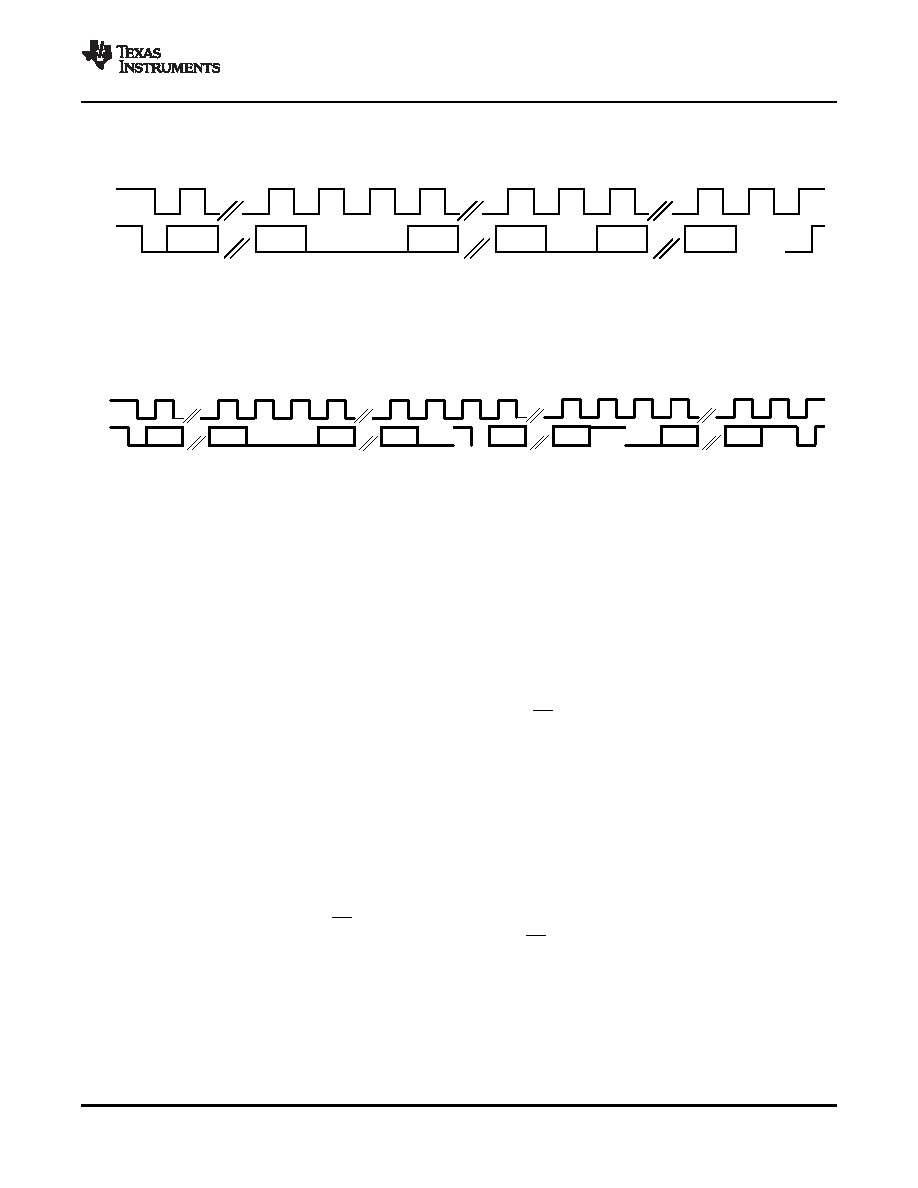
Figure 5-73. I2C Write
Figure 5-74. I2C Read
In the case of an I2C register write, if the master does not issue a STOP condition, then the device enters
auto-increment mode. So in the next eight clocks, the data on SDA is treated as data for the next
incremental register.
Similarly, in the case of an I2C register read, after the device has sent out the 8-bit data from the
addressed register, if the master issues a ACKNOWLEDGE, the slave takes over control of SDA bus and
transmit for the next 8 clocks the data of the next incremental register.
In the SPI control mode, the TSC2117 uses the pins SCLK, SS, MISO, and MOSI as a standard SPI port
with clock polarity setting of 0 (typical microprocessor SPI control bit CPOL = 0). The SPI port allows
full-duplex, synchronous, serial communication between a host processor (the master) and peripheral
devices (slaves). The SPI master (in this case, the host processor) generates the synchronizing clock
(driven onto SCLK) and initiates transmissions. The SPI slave devices (such as the TSC2117) depend on
a master to start and synchronize transmissions. A transmission begins when initiated by an SPI master.
The byte from the SPI master begins shifting in on the slave MOSI pin under the control of the master
serial clock (driven onto SCLK). As the byte shifts in on the MOSI pin, a byte shifts out on the MISO pin to
the master shift register.
The TSC2117 interface is designed so that with a clock-phase bit setting of 1 (typical microprocessor SPI
control bit CPHA = 1), the master begins driving its MOSI pin and the slave begins driving its MISO pin on
the first serial clock edge. The SS pin can remain low between transmissions; however, the TSC2117 only
interprets the first 8 bits transmitted after the falling edge of SS as a command byte, and the next 8 bits as
a data byte only if writing to a register. Reserved register bits should be written to their default values. The
TSC2117 is entirely controlled by registers. Reading and writing these registers is accomplished by an
8-bit command sent to the MOSI pin of the part prior to the data for that register. The command is
structured as shown in Section 5.9.3.3. The first 7 bits specify the register address which is being written
or read, from 0 to 127 (decimal). The command word ends with an R/W bit, which specifies the direction of
APPLICATION INFORMATION
103
相關PDF資料 |
PDF描述 |
|---|---|
| TSC2300IPAGG4 | SPECIALTY CONSUMER CIRCUIT, PQFP64 |
| TSC2300IPAGR | SPECIALTY CONSUMER CIRCUIT, PQFP64 |
| TSC2300IPAG | SPECIALTY CONSUMER CIRCUIT, PQFP64 |
| TSC2300IPAGRG4 | SPECIALTY CONSUMER CIRCUIT, PQFP64 |
| TSC2301IPAGR | SPECIALTY CONSUMER CIRCUIT, PQFP64 |
相關代理商/技術參數 |
參數描述 |
|---|---|
| TSC2117IRGZT | 制造商:Texas Instruments 功能描述:Touch Screen Controller IC |
| TSC22 | 制造商:未知廠家 制造商全稱:未知廠家 功能描述:EURO TERMINAL BLOCKS |
| TSC2200 | 制造商:BB 制造商全稱:BB 功能描述:PDA ANALOG INTERFACE CIRCUIT |
| TSC2200EVM | 功能描述:觸摸傳感器開發工具 Touch Screen Contr Eval Mod RoHS:否 制造商:Cypress Semiconductor 工具用于評估: 接口類型: 工作電壓: 最大工作溫度: |
| TSC2200IPW | 功能描述:觸摸屏轉換器和控制器 Prog 4-Wire w/12-Bit 125KHz ADC & Key Ifc RoHS:否 制造商:Microchip Technology 類型:Resistive Touch Controllers 輸入類型:3 Key 數據速率:140 SPS 分辨率:10 bit 接口類型:4-Wire, 5-Wire, 8-Wire, I2C, SPI 電源電壓:2.5 V to 5.25 V 電源電流:17 mA 工作溫度:- 40 C to + 85 C 封裝 / 箱體:SSOP-20 |
發布緊急采購,3分鐘左右您將得到回復。