- 您現在的位置:買賣IC網 > PDF目錄164976 > A40MX04-VQG80A FPGA, 6000 GATES, PQFP80 PDF資料下載
參數資料
| 型號: | A40MX04-VQG80A |
| 元件分類: | FPGA |
| 英文描述: | FPGA, 6000 GATES, PQFP80 |
| 封裝: | PLASTIC, VQFP-80 |
| 文件頁數: | 44/78頁 |
| 文件大小: | 515K |
| 代理商: | A40MX04-VQG80A |
第1頁第2頁第3頁第4頁第5頁第6頁第7頁第8頁第9頁第10頁第11頁第12頁第13頁第14頁第15頁第16頁第17頁第18頁第19頁第20頁第21頁第22頁第23頁第24頁第25頁第26頁第27頁第28頁第29頁第30頁第31頁第32頁第33頁第34頁第35頁第36頁第37頁第38頁第39頁第40頁第41頁第42頁第43頁當前第44頁第45頁第46頁第47頁第48頁第49頁第50頁第51頁第52頁第53頁第54頁第55頁第56頁第57頁第58頁第59頁第60頁第61頁第62頁第63頁第64頁第65頁第66頁第67頁第68頁第69頁第70頁第71頁第72頁第73頁第74頁第75頁第76頁第77頁第78頁
40MX and 42MX Automotive FPGA Families
v3.0
1-45
Pin Descriptions
CLK/A/B, I/O
Global Clock
Clock inputs for clock distribution networks. CLK is for
40MX while CLKA and CLKB are for 42MX devices. The
clock input is buffered prior to clocking the logic
modules. This pin can also be used as an I/O.
DCLK, I/O
Diagnostic Clock
TTL clock input for diagnostic probe and device
programming. DCLK is active when the MODE pin is
HIGH. This pin functions as an I/O when the MODE pin is
LOW.
GND
Ground
Input LOW supply voltage.
I/O
Input/Output
Input, output, tristate, or bidirectional buffer. Input and
output
levels
are
compatible
with
standard
TTL
specifications. Unused I/O pins are configured by the
Designer software as shown in Table 1-15.
In all cases, it is recommended to tie all unused I/O pins
to LOW on the board. This applies to all dual-purpose
pins when configured as I/Os as well.
MODE
Mode
Controls the use of multifunction pins (DCLK, PRA, PRB,
SDI, TDO). To provide verification capability, the MODE
pin should be held HIGH. To facilitate this, the MODE pin
should be tied to GND through a 10k
resistor so that
the MODE pin can be pulled HIGH when required.
NC
No Connection
This pin is not connected to circuitry within the device.
These pins can be driven to any voltage or can be left
floating with no effect on the operation of the device.
PRA/B, I/O
Probe
The Probe pin is used to output data from any user-
defined design node within the device. Each diagnostic
pin can be used in conjunction with the other probe pin
to allow real-time diagnostic output of any signal path
within the device. The Probe pin can be used as a user-
defined I/O when verification has been completed. The
pin's probe capabilities can be permanently disabled to
protect programmed design confidentiality. The Probe
pin is accessible when the MODE pin is High. This pin
functions as an I/O when the MODE pin is Low.
QCLKA,B,C,D, I/O
Quadrant Clock
Quadrant clock inputs for A42MX36 devices. When not
used as a register control signal, these pins can function
as general-purpose I/Os.
SDI, I/O
Serial Data Input
Serial data input for diagnostic probe and device
programming. SDI is active when the MODE pin is High.
This pin functions as an I/O when the MODE pin is Low.
SDO, TDO, I/O
Serial Data Output
Serial data output for diagnostic probe and device
programming. SDO is active when the MODE pin is High.
This pin functions as an I/O when the MODE pin is Low.
SDO is available for 42MX devices only.
When Silicon Explorer II is being used, SDO will act as an
output while the "checksum" is run. It will return to user
I/O when "checksum" is complete.
TCK, I/O
Test Clock
Clock signal to shift the Boundary Scan Test (BST) data
into the device. This pin functions as an I/O when
"Reserve JTAG" is not checked in the Designer software.
BST pins are only available in the A42MX24 and
A42MX36 devices.
TDI, I/O
Test Data In
Serial data input for BST instructions and data. Data is
shifted in on the rising edge of TCK. This pin functions as
an I/O when "Reserve JTAG" is not checked in the
Designer software. BST pins are only available in the
A42MX24 and A42MX36 devices.
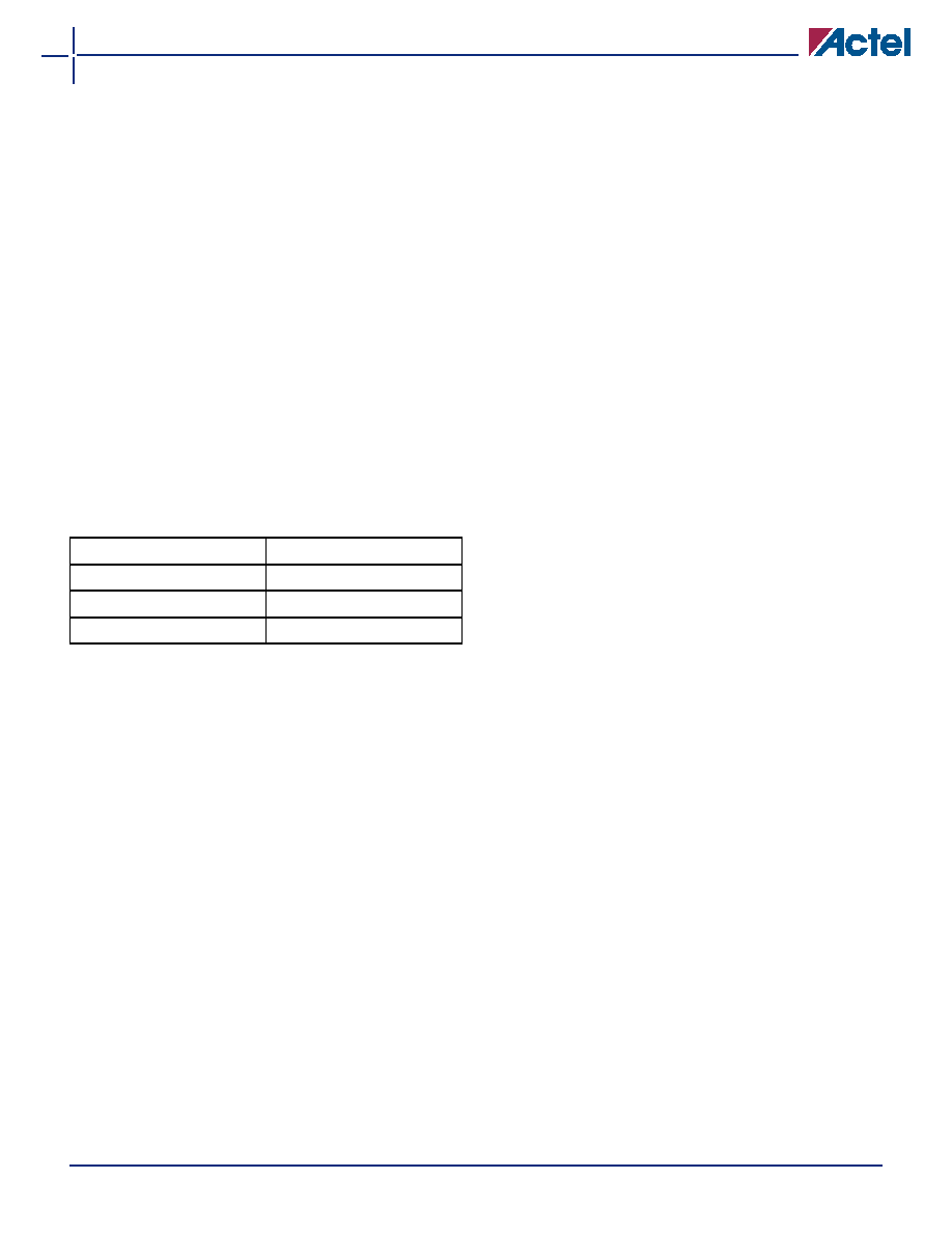
Table 1-15 Configuration of Unused I/Os
Device
Configuration
A40MX02, A40MX04
Pulled LOW
A42MX09, A42MX16
Pulled LOW
A42MX24, A42MX36
Tristated
相關PDF資料 |
PDF描述 |
|---|---|
| A42MX36-1BG272B | FPGA, 2438 CLBS, 36000 GATES, PBGA272 |
| A42MX36-1BGG272B | FPGA, 2438 CLBS, 36000 GATES, PBGA272 |
| A42MX36-1PQ208B | FPGA, 2438 CLBS, 36000 GATES, PQFP208 |
| A42MX36-1PQ240B | FPGA, 2438 CLBS, 36000 GATES, PQFP240 |
| A42MX36-1PQG208B | FPGA, 2438 CLBS, 36000 GATES, PQFP208 |
相關代理商/技術參數 |
參數描述 |
|---|---|
| A40MX04-VQG80I | 功能描述:IC FPGA MX SGL CHIP 6K 80-VQFP RoHS:是 類別:集成電路 (IC) >> 嵌入式 - FPGA(現場可編程門陣列) 系列:MX 標準包裝:90 系列:ProASIC3 LAB/CLB數:- 邏輯元件/單元數:- RAM 位總計:36864 輸入/輸出數:157 門數:250000 電源電壓:1.425 V ~ 1.575 V 安裝類型:表面貼裝 工作溫度:-40°C ~ 125°C 封裝/外殼:256-LBGA 供應商設備封裝:256-FPBGA(17x17) |
| A40MX04-VQG80M | 制造商:Microsemi Corporation 功能描述:FPGA 6K GATES 547 CELLS 83MHZ/139MHZ 0.45UM 3.3V/5V 80VQFP - Trays 制造商:Microsemi Corporation 功能描述:IC FPGA MX SGL CHIP 6K 80-VQFP 制造商:Microsemi Corporation 功能描述:IC FPGA 69 I/O 80VQFP |
| A40MX09-PL84 | 制造商:Microsemi SOC Products Group 功能描述: |
| A40P24 | 制造商:Pentair Technical Products / Hoffman 功能描述:Panel 37.00x21.00 fits 40.00x2 White, fits 40x24, Steel |
| A-40P24 | 制造商:Pentair Technical Products / Hoffman 功能描述:Panel 37.00x21.00 fits 40.00x2 制造商:PENTAIR TECNICAL PRODCUTS 功能描述:Panel 37.00x21.00 fits 40.00x2 |
發布緊急采購,3分鐘左右您將得到回復。