- 您現在的位置:買賣IC網 > PDF目錄373970 > AD9923ABBCZ (ANALOG DEVICES INC) CCD Signal Processor with V-Driver and Precision Timing⑩ Generator PDF資料下載
參數資料
| 型號: | AD9923ABBCZ |
| 廠商: | ANALOG DEVICES INC |
| 元件分類: | 消費家電 |
| 英文描述: | CCD Signal Processor with V-Driver and Precision Timing⑩ Generator |
| 中文描述: | SPECIALTY CONSUMER CIRCUIT, PBGA105 |
| 封裝: | 8 X 8 MM, 0.65 MM PITCH, ROHS COMPLIANT, MO-225, CSPBGA-105 |
| 文件頁數: | 1/88頁 |
| 文件大小: | 852K |
| 代理商: | AD9923ABBCZ |
當前第1頁第2頁第3頁第4頁第5頁第6頁第7頁第8頁第9頁第10頁第11頁第12頁第13頁第14頁第15頁第16頁第17頁第18頁第19頁第20頁第21頁第22頁第23頁第24頁第25頁第26頁第27頁第28頁第29頁第30頁第31頁第32頁第33頁第34頁第35頁第36頁第37頁第38頁第39頁第40頁第41頁第42頁第43頁第44頁第45頁第46頁第47頁第48頁第49頁第50頁第51頁第52頁第53頁第54頁第55頁第56頁第57頁第58頁第59頁第60頁第61頁第62頁第63頁第64頁第65頁第66頁第67頁第68頁第69頁第70頁第71頁第72頁第73頁第74頁第75頁第76頁第77頁第78頁第79頁第80頁第81頁第82頁第83頁第84頁第85頁第86頁第87頁第88頁
CCD Signal Processor with V-Driver and
Precision Timing
Generator
AD9923A
FEATURES
Integrated 15-channel V-driver
12-bit, 36 MHz analog-to-digital converter (ADC)
Similar register map to the AD9923
5-field, 10-phase vertical clock support
Complete on-chip timing generator
Precision Timing
core with <600 ps resolution
Correlated double sampler (CDS)
6 dB to 42 dB 10-bit variable gain amplifier (VGA)
Black level clamp with variable level control
On-chip 3 V horizontal and RG drivers
2-phase and 4-phase H-clock modes
Electronic and mechanical shutter support
On-chip driver for external crystal
On-chip sync generator with external sync input
8 mm × 8 mm CSP_BGA package with 0.65 mm pitch
Rev. 0
Information furnished by Analog Devices is believed to be accurate and reliable. However, no
responsibility is assumed by Analog Devices for its use, nor for any infringements of patents or other
rights of third parties that may result from its use. Specifications subject to change without notice. No
license is granted by implication or otherwise under any patent or patent rights of Analog Devices.
Trademarks and registered trademarks are the property of their respective owners.
One Technology Way, P.O. Box 9106, Norwood, MA 02062-9106, U.S.A.
Tel: 781.329.4700
Fax: 781.461.3113
2006 Analog Devices, Inc. All rights reserved.
www.analog.com
APPLICATIONS
Digital still cameras
.
GENERAL DESCRIPTION
The AD9923A is a complete 36 MHz front-end solution for
digital still cameras and other CCD imaging applications.
Similar to the AD9923 product, the AD9923A includes the
analog front end (AFE), a fully programmable timing generator
(TG), and a 15-channel vertical driver (V-driver). A
Precision
Timing
core allows adjustment of high speed clocks with
approximately 600 ps resolution at 36 MHz operation.
The on-chip V-driver supports up to 15 channels for use with
5-field, 10-phase CCDs.
The analog front end includes black level clamping, CDS, VGA,
and a 12-bit ADC. The timing generator and V-driver provide
all the necessary CCD clocks: RG, H-clocks, vertical clocks, sensor
gate pulses, substrate clock, and substrate bias control. The
internal registers are programmed using a 3-wire serial
interface.
Packaged in an 8 mm × 8 mm CSP_BGA, the AD9923A is
specified over an operating temperature range of 25°C to +85°C.
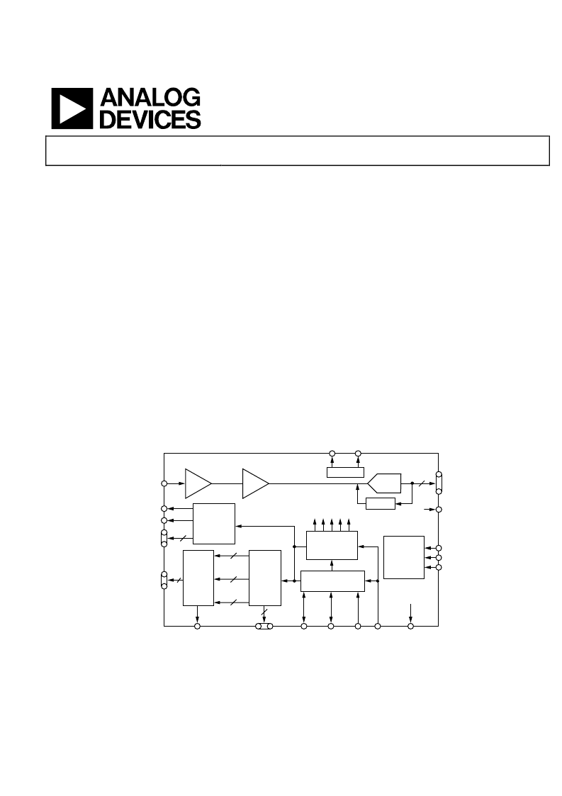
FUNCTIONAL BLOCK DIAGRAM
AD9923A
DCLK
CLAMP
D0 TO D11
CCDIN
12-BIT
ADC
–3dB, 0dB, +3dB, +6dB
CDS
12
REFT
REFB
VREF
+6dB TO +42dB
VGA
HORIZONTAL
DRIVERS
RG
HL
H1 TO H4
4
INTERNAL
REGISTERS
SL
SDI
SCK
SYNC
GENERATOR
PRECISION
TIMING
GENERATOR
INTERNAL CLOCKS
HD
VD
SYNC
CLI
CLO
VSUB, MSHUT,
STROBE
SUBCK
VERTICAL
TIMING
CONTROL
V-DRIVER
V1, V2, V3,
V4, V5A, V5B,
V6, V7A, V7B,
V8, V9, V10,
V11, V12, V13
15
3
XSUBCK,
XSUBCNT
2
XSG1 TO
XSG8
8
XV1 TO
XV13
13
0
Figure 1.
相關PDF資料 |
PDF描述 |
|---|---|
| AD9923ABBCZRL | CCD Signal Processor with V-Driver and Precision Timing⑩ Generator |
| AD9925BBCZRL | CCD Signal Processor with Vertical Driver and Precision Timing Generator |
| AD9925 | CCD Signal Processor with Vertical Driver and Precision Timing Generator |
| AD9925BBCZ | CCD Signal Processor with Vertical Driver and Precision Timing Generator |
| AD9927 | 14-Bit CCD Signal Processor with V-Driver and Precision TimingTM Generator |
相關代理商/技術參數 |
參數描述 |
|---|---|
| AD9923ABBCZRL | 功能描述:IC PROCESSOR CCD 12BIT 105CSPBGA RoHS:是 類別:集成電路 (IC) >> 接口 - 傳感器和探測器接口 系列:- 其它有關文件:Automotive Product Guide 產品培訓模塊:Lead (SnPb) Finish for COTS Obsolescence Mitigation Program 標準包裝:74 系列:- 類型:觸控式傳感器 輸入類型:數字 輸出類型:數字 接口:JTAG,串行 電流 - 電源:100µA 安裝類型:表面貼裝 封裝/外殼:20-TSSOP(0.173",4.40mm 寬) 供應商設備封裝:20-TSSOP 包裝:管件 |
| AD9923BBCZ | 制造商:Rochester Electronics LLC 功能描述:- Bulk 制造商:Analog Devices 功能描述: |
| AD9923BBCZRL | 制造商:Rochester Electronics LLC 功能描述: 制造商:Analog Devices 功能描述: |
| AD9924BBCZ | 制造商:Analog Devices 功能描述: |
| AD9924BBCZRL | 制造商:Rochester Electronics LLC 功能描述:- Bulk |
發布緊急采購,3分鐘左右您將得到回復。