- 您現在的位置:買賣IC網 > PDF目錄382345 > MPC9600 (Motorola, Inc.) LOW VOLTAGE 2.5 V AND 3.3 V CMOS PLL CLOCK DRIVER PDF資料下載
參數資料
| 型號: | MPC9600 |
| 廠商: | Motorola, Inc. |
| 英文描述: | LOW VOLTAGE 2.5 V AND 3.3 V CMOS PLL CLOCK DRIVER |
| 中文描述: | 低電壓2.5 V和3.3 V的CMOS PLL時鐘驅動器 |
| 文件頁數: | 7/16頁 |
| 文件大小: | 321K |
| 代理商: | MPC9600 |
TIMING SOLUTIONS
MOTOROLA
APPLICATIONS INFORMATION
Programming the MPC9600
The MPC9600 clock driver outputs can be configured into
several divider modes. Additionally the external feedback of
the device allows for flexibility in establishing various input to
output frequency relationships. The selectable feedback
divider of the three output groups allows the user to configure
the device for 1:2, 1:3, 1:4 and 1:6 input:output frequency
ratios. The use of even dividers ensure that the output duty
cycle is always 50%. Table 6 illustrates the various output
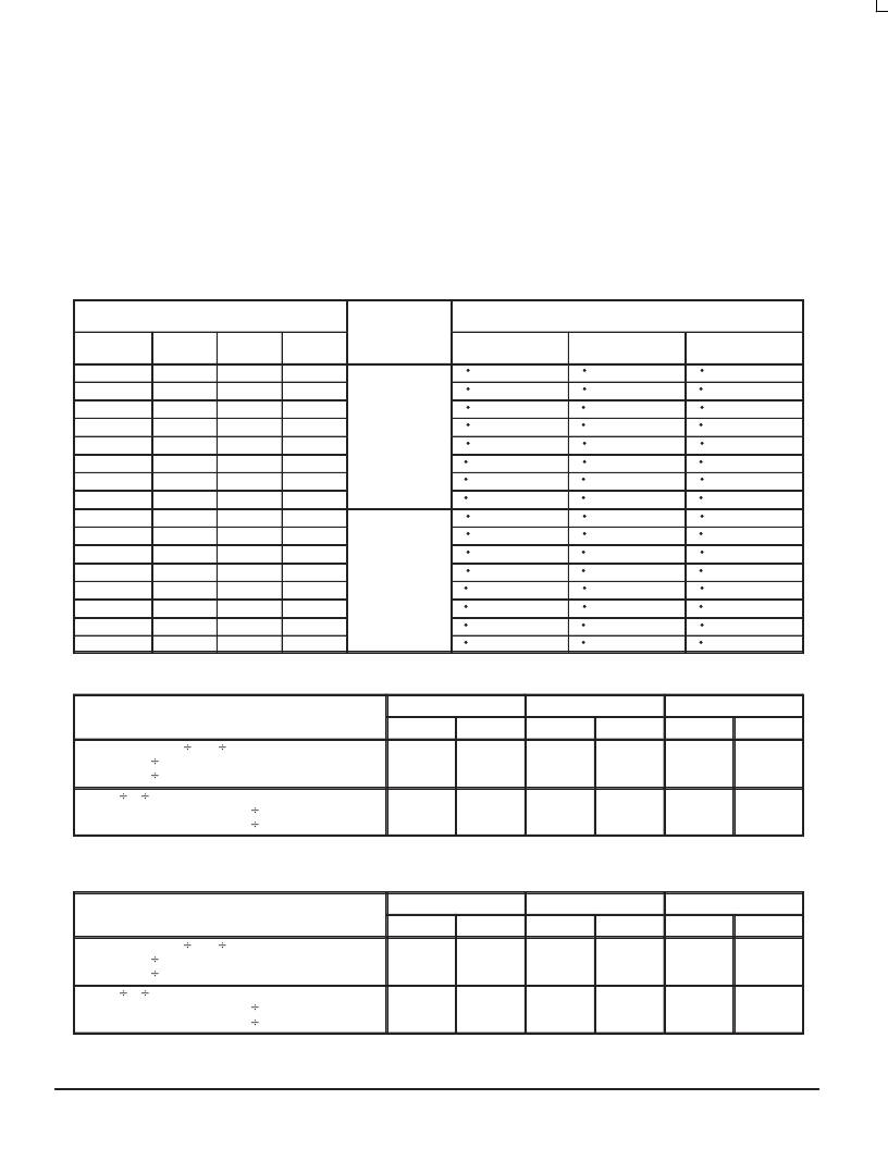
Table 6: Output Frequency Relationshipa for QFB connected to FB_IN
configurations, the table describes the outputs using the
input clock frequency CLK as a reference.
The feedback divider division settings establish the output
relationship, in addition, it must be ensured that the VCO will
be stable given the frequency of the outputs desired. The
feedback frequency should be used to situate the VCO into a
frequency range in which the PLL will be stable. The design
of the PLL supports output frequencies from 50 MHz to 200
MHz while the VCO frequency range is specified from 200
MHz to 400 MHz and should not be exceeded for stable
operation.
Configuration Inputs
Input
Frequency
Range CLK
[MHz]
Output Frequency Ratio and Range
FSEL_FB
FSELA
FSELB
FSELC
Ratio, QAx [MHz]
Ratio, QBx [MHz]
Ratio, QCx [MHz]
0
0
0
0
0
0
0
0
1
1
1
1
1
1
1
1
0
0
0
0
1
1
1
1
0
0
0
0
1
1
1
1
0
0
1
1
0
0
1
1
0
0
1
1
0
0
1
1
0
1
0
1
0
1
0
1
0
1
0
1
0
1
0
1
4 CLK (100–200)
4 CLK (100–200)
4 CLK (100–200)
4 CLK (100–200)
2 CLK (50.0–100)
2 CLK (50.0–100)
2 CLK (50.0–100)
2 CLK (50.0–100)
6 CLK (100–200)
6 CLK (100–200)
6 CLK (100–200)
6 CLK (100–200)
3 CLK (50.0–100)
3 CLK (50.0–100)
3 CLK (50.0–100)
3 CLK (50.0–100)
4 CLK (100–200)
4 CLK (100–200)
2 CLK (50.0–100)
2 CLK (50.0–100)
4 CLK (100–200)
4 CLK (100–200)
2 CLK (50.0–100)
2 CLK (50.0–100)
6 CLK (100–200)
6 CLK (100–200)
3 CLK (50.0–100)
3 CLK (50.0–100)
6 CLK (100–200)
6 CLK (100–200)
3 CLK (50.0–100)
3 CLK (50.0–100)
4 CLK (100–200)
2 CLK (50.0–100)
4 CLK (100–200)
2 CLK (50.0–100)
4 CLK (100–200)
2 CLK (50.0–100)
4 CLK (100–200)
2 CLK (50.0–100)
6 CLK (100–200)
3 CLK (50.0–100)
6 CLK (100–200)
3 CLK (50.0–100)
6 CLK (100–200)
3 CLK (50.0–100)
6 CLK (100–200)
3 CLK (50.0–100)
25.0–50.0
16.67–33.33
a. Output frequency relationship with respect to input reference frequency CLK. The VCO frequency range is always 200–400.
Typical and Maximum Period Jitter Specification
Device Configuration
QA0 to QA6
QB0 to QB6
QC0 to QC6
Typ
Max
Typ
Max
Typ
Max
All output banks in
2 or
4 divider configurationa
2 (FSELA=0 and FESLB=0 and FSELC=0)
4 (FSELA=1 and FESLB=1 and FSELC=1)
4 divider configurationsb
for output banks in
2 divider configurations
for output banks in
4 divider configurations
25
20
50
70
50
50
70
100
25
20
50
70
Mixed
2/
80
25
130
70
100
60
150
100
80
25
130
70
a. In this configuration, all MPC9600 outputs generate the same clock frequency. See Figure 1 for an example configuration.
b. Multiple frequency generation. Jitter data are specified for each output divider sepeerately. See Figure 2 for an example.
Typical and Maximum Cycle–to–cycle Jitter Specification
Device Configuration
QA0 to QA6
QB0 to QB6
QC0 to QC6
Typ
Max
Typ
Max
Typ
Max
All output banks in
2 or
4 divider configurationa
2 (FSELA=0 and FESLB=0 and FSELC=0)
4 (FSELA=1 and FESLB=1 and FSELC=1)
4 divider configurationsb
for output banks in
2 divider configurations
for output banks in
4 divider configurations
40
40
90
110
80
120
130
180
40
40
90
110
Mixed
2/
150
30
250
110
200
120
280
180
150
30
250
110
a. In this configuration, all MPC9600 outputs generate the same clock frequency.
b. Multiple frequency generation. Jitter data are specified for each output divider sepeerately.
F
Freescale Semiconductor, Inc.
For More Information On This Product,
Go to: www.freescale.com
n
.
相關PDF資料 |
PDF描述 |
|---|---|
| MPC9772 | 3.3V 1:12 LVCMOS PLL Clock Generator |
| MPC9893 | Low Voltage PLL Intelligent Dynamic Clock (IDCS) Switch |
| MPC99J93 | Intelligent Dynamic Clock Switch (IDCS) PLL Clock Driver |
| MPD-425V | 250W DC-DC POWER SUPPLY INPUT RANGE: 40~57VDC |
| MPE-902M | SWITCHING POWER SUPPLY |
相關代理商/技術參數 |
參數描述 |
|---|---|
| MPC9600AE | 功能描述:時鐘發生器及支持產品 RoHS:否 制造商:Silicon Labs 類型:Clock Generators 最大輸入頻率:14.318 MHz 最大輸出頻率:166 MHz 輸出端數量:16 占空比 - 最大:55 % 工作電源電壓:3.3 V 工作電源電流:1 mA 最大工作溫度:+ 85 C 安裝風格:SMD/SMT 封裝 / 箱體:QFN-56 |
| MPC9600AER2 | 功能描述:時鐘緩沖器 RoHS:否 制造商:Texas Instruments 輸出端數量:5 最大輸入頻率:40 MHz 傳播延遲(最大值): 電源電壓-最大:3.45 V 電源電壓-最小:2.375 V 最大功率耗散: 最大工作溫度:+ 85 C 最小工作溫度:- 40 C 封裝 / 箱體:LLP-24 封裝:Reel |
| MPC9600FA | 功能描述:IC CLOCK DRVR PLL LV 1:21 48LQFP RoHS:否 類別:集成電路 (IC) >> 時鐘/計時 - 時鐘發生器,PLL,頻率合成器 系列:- 標準包裝:39 系列:- 類型:* PLL:帶旁路 輸入:時鐘 輸出:時鐘 電路數:1 比率 - 輸入:輸出:1:10 差分 - 輸入:輸出:是/是 頻率 - 最大:170MHz 除法器/乘法器:無/無 電源電壓:2.375 V ~ 3.465 V 工作溫度:0°C ~ 70°C 安裝類型:* 封裝/外殼:* 供應商設備封裝:* 包裝:* |
| MPC9608 | 制造商:MOTOROLA 制造商全稱:Motorola, Inc 功能描述:1:10 LVCMOS Zero Delay Clock Buffer |
| MPC9608AC | 功能描述:時鐘緩沖器 RoHS:否 制造商:Texas Instruments 輸出端數量:5 最大輸入頻率:40 MHz 傳播延遲(最大值): 電源電壓-最大:3.45 V 電源電壓-最小:2.375 V 最大功率耗散: 最大工作溫度:+ 85 C 最小工作溫度:- 40 C 封裝 / 箱體:LLP-24 封裝:Reel |
發布緊急采購,3分鐘左右您將得到回復。