- 您現(xiàn)在的位置:買(mǎi)賣(mài)IC網(wǎng) > PDF目錄382345 > MPC9600 (Motorola, Inc.) LOW VOLTAGE 2.5 V AND 3.3 V CMOS PLL CLOCK DRIVER PDF資料下載
參數(shù)資料
| 型號(hào): | MPC9600 |
| 廠商: | Motorola, Inc. |
| 英文描述: | LOW VOLTAGE 2.5 V AND 3.3 V CMOS PLL CLOCK DRIVER |
| 中文描述: | 低電壓2.5 V和3.3 V的CMOS PLL時(shí)鐘驅(qū)動(dòng)器 |
| 文件頁(yè)數(shù): | 9/16頁(yè) |
| 文件大小: | 321K |
| 代理商: | MPC9600 |
第1頁(yè)第2頁(yè)第3頁(yè)第4頁(yè)第5頁(yè)第6頁(yè)第7頁(yè)第8頁(yè)當(dāng)前第9頁(yè)第10頁(yè)第11頁(yè)第12頁(yè)第13頁(yè)第14頁(yè)第15頁(yè)第16頁(yè)
TIMING SOLUTIONS
MOTOROLA
Using the MPC9600 in zero–delay applications
Nested clock trees are typical applications for the
MPC9600. For these applications the MPC9600 offers a
differential LVPECL clock input pair as a PLL reference. This
allows for the use of differential LVPECL primary clock
distribution devices such as the Motorola MC100ES6111 or
MC100ES6226, taking advantage of its superior low-skew
performance. Clock trees using LVPECL for clock distribution
and the MPC9600 as LVCMOS PLL fanout buffer with zero
insertion delay will show significantly lower clock skew than
clock distributions developed from CMOS fanout buffers.
The external feedback option of the MPC9600 PLL allows
for its use as a zero delay buffer. The PLL aligns the feedback
clock output edge with the clock input reference edge and
virtually eliminates the propagation delay through the device.
The remaining insertion delay (skew error) of the
MPC9600 in zero-delay applications is measured between
the reference clock input and any output. This effective delay
consists of the static phase offset (SPO or t(
)), I/O jitter
(tJIT(
), phase or long-term jitter), feedback path delay and
the output-to-output skew (tSK(O) relative to the feedback
output.
Calculation of part-to-part skew
The MPC9600 zero delay buffer supports applications
where critical clock signal timing can be maintained across
several devices. If the reference clock inputs (CCLK or
PCLK) of two or more MPC9600 are connected together, the
maximum overall timing uncertainty from the common CCLK
input to any output is:
tSK(PP) = t(
) + tSK(O) + tPD, LINE(FB) + tJIT(
) CF
This maximum timing uncertainty consist of 4
components: static phase offset, output skew, feedback
board trace delay and I/O (phase) jitter:
Figure 6. MPC9600 max. device-to-device skew
tPD,LINE(FB)
tJIT(
)
+
t
SK(O)
–t(
)
+t(
)
tJIT(
)
+
t
SK(O)
tSK(PP)
Max. skew
TCLKCommon
QFBDevice 1
Any QDevice 1
QFBDevice2
Any QDevice 2
Due to the statistical nature of I/O jitter a RMS value (1 )
is specified. I/O jitter numbers for other confidence factors
(CF) can be derived from Table 8.
Table 8: Confidence Facter CF
CF
Probability of clock edge within the distribution
±
1
±
2
±
3
±
4
±
5
±
6
0.68268948
0.95449988
0.99730007
0.99993663
0.99999943
0.99999999
The feedback trace delay is determined by the board
layout and can be used to fine-tune the effective delay
through each device. In the following example calculation a
I/O jitter confidence factor of 99.7% (
±
3 ) is assumed,
resulting in a worst case timing uncertainty from input to any
output of -261 ps to 341 ps relative to CCLK (VCC=3.3V and
fVCO = 200 MHz):
tSK(PP) =
[–60ps...140ps] + [–150ps...150ps] +
[(17ps –3)...(17ps 3)] + tPD, LINE(FB)
[–261ps...341ps] + tPD, LINE(FB)
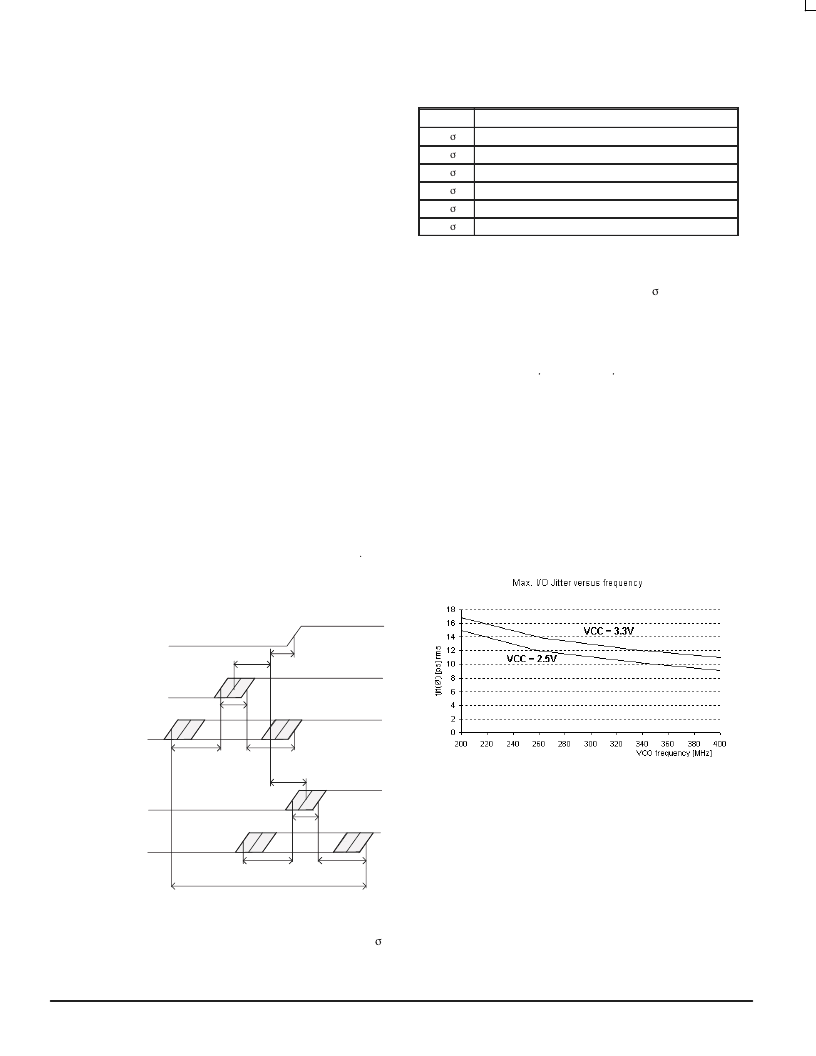
Above equation uses the maximum I/O jitter number
shown in the AC characteristic table for VCC=3.3V (17 ps
RMS). I/O jitter is frequency dependant with a maximum at
the lowest VCO frequency (200 MHz for the MPC9600).
Applications using a higher VCO frequency exhibit less I/O
jitter than the AC characteristic limit. The I/O jitter
characteristics in Figure 7. can be used to derive a smaller
I/O jitter number at the specific VCO frequency, resulting in
tighter timing limits in zero-delay mode and for part-to-part
skew tSK(PP).
tSK(PP) =
Figure 7. Max. I/O Jitter versus VCO frequency for
VCC=2.5V and VCC=3.3V
Driving Transmission Lines
The MPC9600 clock driver was designed to drive high
speed signals in a terminated transmission line environment.
To provide the optimum flexibility to the user the output
drivers were designed to exhibit the lowest impedance
possible. With an output impedance of less than 20
the
drivers can drive either parallel or series terminated
transmission lines. For more information on transmission
lines the reader is referred to Motorola application note
AN1091. In most high performance clock networks
point-to-point distribution of signals is the method of choice.
In a point-to-point scheme either series terminated or parallel
F
Freescale Semiconductor, Inc.
For More Information On This Product,
Go to: www.freescale.com
n
.
相關(guān)PDF資料 |
PDF描述 |
|---|---|
| MPC9772 | 3.3V 1:12 LVCMOS PLL Clock Generator |
| MPC9893 | Low Voltage PLL Intelligent Dynamic Clock (IDCS) Switch |
| MPC99J93 | Intelligent Dynamic Clock Switch (IDCS) PLL Clock Driver |
| MPD-425V | 250W DC-DC POWER SUPPLY INPUT RANGE: 40~57VDC |
| MPE-902M | SWITCHING POWER SUPPLY |
相關(guān)代理商/技術(shù)參數(shù) |
參數(shù)描述 |
|---|---|
| MPC9600AE | 功能描述:時(shí)鐘發(fā)生器及支持產(chǎn)品 RoHS:否 制造商:Silicon Labs 類(lèi)型:Clock Generators 最大輸入頻率:14.318 MHz 最大輸出頻率:166 MHz 輸出端數(shù)量:16 占空比 - 最大:55 % 工作電源電壓:3.3 V 工作電源電流:1 mA 最大工作溫度:+ 85 C 安裝風(fēng)格:SMD/SMT 封裝 / 箱體:QFN-56 |
| MPC9600AER2 | 功能描述:時(shí)鐘緩沖器 RoHS:否 制造商:Texas Instruments 輸出端數(shù)量:5 最大輸入頻率:40 MHz 傳播延遲(最大值): 電源電壓-最大:3.45 V 電源電壓-最小:2.375 V 最大功率耗散: 最大工作溫度:+ 85 C 最小工作溫度:- 40 C 封裝 / 箱體:LLP-24 封裝:Reel |
| MPC9600FA | 功能描述:IC CLOCK DRVR PLL LV 1:21 48LQFP RoHS:否 類(lèi)別:集成電路 (IC) >> 時(shí)鐘/計(jì)時(shí) - 時(shí)鐘發(fā)生器,PLL,頻率合成器 系列:- 標(biāo)準(zhǔn)包裝:39 系列:- 類(lèi)型:* PLL:帶旁路 輸入:時(shí)鐘 輸出:時(shí)鐘 電路數(shù):1 比率 - 輸入:輸出:1:10 差分 - 輸入:輸出:是/是 頻率 - 最大:170MHz 除法器/乘法器:無(wú)/無(wú) 電源電壓:2.375 V ~ 3.465 V 工作溫度:0°C ~ 70°C 安裝類(lèi)型:* 封裝/外殼:* 供應(yīng)商設(shè)備封裝:* 包裝:* |
| MPC9608 | 制造商:MOTOROLA 制造商全稱(chēng):Motorola, Inc 功能描述:1:10 LVCMOS Zero Delay Clock Buffer |
| MPC9608AC | 功能描述:時(shí)鐘緩沖器 RoHS:否 制造商:Texas Instruments 輸出端數(shù)量:5 最大輸入頻率:40 MHz 傳播延遲(最大值): 電源電壓-最大:3.45 V 電源電壓-最小:2.375 V 最大功率耗散: 最大工作溫度:+ 85 C 最小工作溫度:- 40 C 封裝 / 箱體:LLP-24 封裝:Reel |
發(fā)布緊急采購(gòu),3分鐘左右您將得到回復(fù)。