- 您現在的位置:買賣IC網 > PDF目錄98215 > TFP6424PAP (TEXAS INSTRUMENTS INC) SPECIALTY CONSUMER CIRCUIT, PQFP64 PDF資料下載
參數資料
| 型號: | TFP6424PAP |
| 廠商: | TEXAS INSTRUMENTS INC |
| 元件分類: | 消費家電 |
| 英文描述: | SPECIALTY CONSUMER CIRCUIT, PQFP64 |
| 封裝: | 10 X 10 MM, 1.40 MM HEIGHT, 0.50 MM PITCH, THERMALLY ENHANCED, POWER, PLASTIC, TQFP-64 |
| 文件頁數: | 2/65頁 |
| 文件大小: | 813K |
| 代理商: | TFP6424PAP |
第1頁當前第2頁第3頁第4頁第5頁第6頁第7頁第8頁第9頁第10頁第11頁第12頁第13頁第14頁第15頁第16頁第17頁第18頁第19頁第20頁第21頁第22頁第23頁第24頁第25頁第26頁第27頁第28頁第29頁第30頁第31頁第32頁第33頁第34頁第35頁第36頁第37頁第38頁第39頁第40頁第41頁第42頁第43頁第44頁第45頁第46頁第47頁第48頁第49頁第50頁第51頁第52頁第53頁第54頁第55頁第56頁第57頁第58頁第59頁第60頁第61頁第62頁第63頁第64頁第65頁
TFP6422, TFP6424
PanelBus
DIGITAL TRANSMITTER/VIDEO ENCODER COMBO
SLDS118 – MARCH 2000
10
POST OFFICE BOX 655303
DALLAS, TEXAS 75265
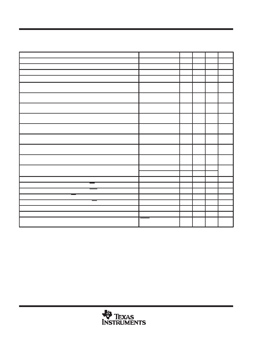
electrical characteristics over recommended operating free-air temperature range (unless
otherwise noted) (continued)
ac specifications
PARAMETER
TEST CONDITIONS
MIN
TYP
MAX
UNIT
VID
Differential input sensitivity
150
1560
mVp-p
t(1)
Analog input intra-pair (+ to -) differential skew time
0.4
tbit
t(2)
Analog Input inter-pair or channel-to-channel skew time
1
tpix§
t(3)
Worse case differential input clock jitter tolerance
TBD
ns
tr(1)
Rise time of data and control signals#, ||
ST = Low,
CL=5 pF
ST = High,
CL=10 pF
2.9
3.1
ns
tf(1)
Fall time of data and control signals#, ||
ST = Low,
CL=5 pF
ST = High,
CL=10 pF
2.84
3.2
ns
tr(2)
Rise time of ODCK clock#
ST = Low,
CL=5 pF
ST = High,
CL=10 pF
TBD
ns
tf(2)
Fall time of ODCK clock#
ST = Low,
CL=5 pF
ST = High,
CL=10 pF
TBD
ns
tsu(1)
Setup time, data and control signal to falling edge of ODCK
(OCK_INV = low)||
ST = Low,
CL=5 pF
ST = High,
CL=10 pF
TBD
ns
th(1)
Hold time, data and control signal to falling edge of ODCK
(OCK_INV = low)||
ST = Low,
CL=5 pF
ST = High,
CL=10 pF
TBD
ns
tsu(2)
Setup time, data and control signal to rising edge of ODCK
(OCK_INV = high)||
ST = Low,
CL=5 pF
ST = High,
CL=10 pF
TBD
ns
th(2)
Hold time, data and control signal to rising edge of ODCK
(OCK_INV = high)||
ST = Low,
CL=5 pF
ST = High,
CL=10 pF
TBD
ns
f(ODCK)
ODCK frequency
PIX = Low (1-PIX/CLK)
25
112
MHz
f(ODCK)
ODCK frequency
PIX = High (2-PIX/CLK)
12.5
56
MHz
ODCK duty-cycle
40%
50%
60%
td(1)
Propagation delay time from PD low to Hi-Z outputs
9
ns
td(2)
Propagation delay time from PDO low to Hi-Z outputs
9
ns
td(3)
Delay time from PD rising edge to inputs active
ns
td(4)
Pulse duration, minimum time PD low
ns
tt(1)
Transition time between DE transition to SCDT lowk
1e6
tpix
tt(2)
Transition time between DE transition to SCDT highk
1280
tpix
ts(1)
Delay time, ODCK latching edge to QE[23:0] data output
STAG = Low,
Pixs = High
0.25
tpix
Specified as ac parameter to include sensitivity to overshoot, undershoot and reflection.
tbit is 1/10 the pixel time, tpix
§ tpix is the pixel time defined as the period of the RxC input clock. The period of ODCK is equal to tpix in 1-pixel/clock mode or 2tpix when in
2-pixel/clock mode.
Measured differentially at 50% crossing using ODCK output clock as trigger.
# Rise and fall times measured as time between 20% and 80% of signal amplitude.
|| Data and control signals are : QE[23:0], QO[23:0], DE, HSYNC, VSYNC and CTL[3:1]
kLink active or inactive is determined by amount of time detected between DE transitions. SCDT indicates link activity.
PRODUCT
PREVIEW
相關PDF資料 |
PDF描述 |
|---|---|
| TFP9431CPAP | SPECIALTY CONSUMER CIRCUIT, PQFP64 |
| TG355ENK-7916 | 8.15 MHz, LOW PASS FILTER |
| TH355BDI-4957 | 4.43 MHz, BAND PASS FILTER |
| TH355LDK-7915 | 8.15 MHz, LOW PASS FILTER |
| TH355LNK-4550 | 10 MHz, LOW PASS FILTER |
相關代理商/技術參數 |
參數描述 |
|---|---|
| TFP70N06 | 制造商:TAK_CHEONG 制造商全稱:Tak Cheong Electronics (Holdings) Co.,Ltd 功能描述:N-Channel Power MOSFET 70A, 60V, 0.014Ω |
| TFP730 | 制造商:TAK_CHEONG 制造商全稱:Tak Cheong Electronics (Holdings) Co.,Ltd 功能描述:N-Channel Power MOSFET 5.5A, 400V, 0.95Ω |
| TFP740 | 制造商:TAK_CHEONG 制造商全稱:Tak Cheong Electronics (Holdings) Co.,Ltd 功能描述:N-Channel Power MOSFET 10A, 400V, 0.55Ω |
| TFP7433PZP | 制造商:Texas Instruments 功能描述: |
| TFP7445PZP-6 | 制造商:Texas Instruments 功能描述: |
發布緊急采購,3分鐘左右您將得到回復。