- 您現在的位置:買賣IC網 > PDF目錄98215 > TFP6424PAP (TEXAS INSTRUMENTS INC) SPECIALTY CONSUMER CIRCUIT, PQFP64 PDF資料下載
參數資料
| 型號: | TFP6424PAP |
| 廠商: | TEXAS INSTRUMENTS INC |
| 元件分類: | 消費家電 |
| 英文描述: | SPECIALTY CONSUMER CIRCUIT, PQFP64 |
| 封裝: | 10 X 10 MM, 1.40 MM HEIGHT, 0.50 MM PITCH, THERMALLY ENHANCED, POWER, PLASTIC, TQFP-64 |
| 文件頁數: | 45/65頁 |
| 文件大小: | 813K |
| 代理商: | TFP6424PAP |
第1頁第2頁第3頁第4頁第5頁第6頁第7頁第8頁第9頁第10頁第11頁第12頁第13頁第14頁第15頁第16頁第17頁第18頁第19頁第20頁第21頁第22頁第23頁第24頁第25頁第26頁第27頁第28頁第29頁第30頁第31頁第32頁第33頁第34頁第35頁第36頁第37頁第38頁第39頁第40頁第41頁第42頁第43頁第44頁當前第45頁第46頁第47頁第48頁第49頁第50頁第51頁第52頁第53頁第54頁第55頁第56頁第57頁第58頁第59頁第60頁第61頁第62頁第63頁第64頁第65頁
TFP6422, TFP6424
PanelBus
DIGITAL TRANSMITTER/VIDEO ENCODER COMBO
SLDS118 – MARCH 2000
5
POST OFFICE BOX 655303
DALLAS, TEXAS 75265
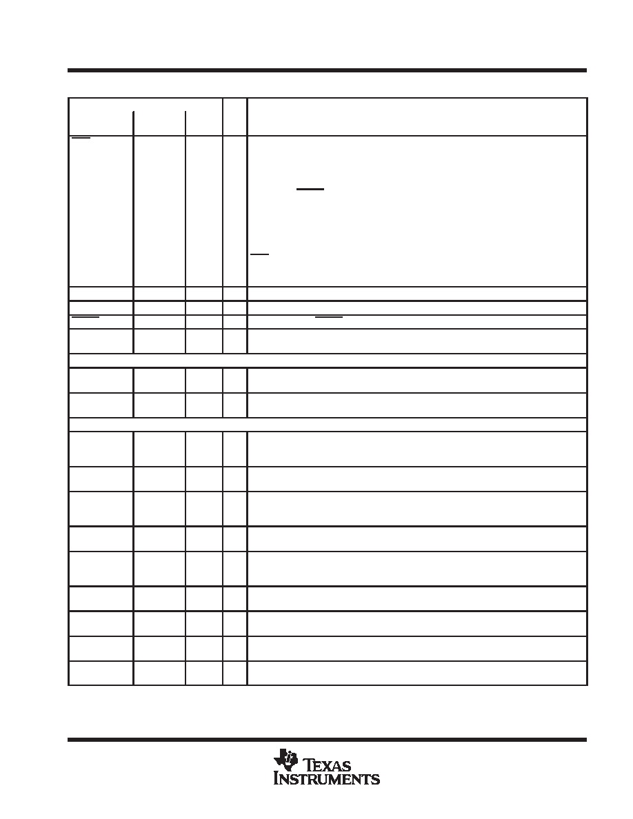
Terminal Functions (Continued)
TERMINAL
NAME
POWER
RAIL
NO.
I/O
DESCRIPTION
INT1/CLKOUT
DVDD
7
O
This pin can be programmed as clock or interrupt output.
Clock out – The internal TV encoder PLL drives CLKOUT. The frequency of CLKOUT is
programmable and depends on TV standards, and the desired horizontal and vertical
overscan compensation ratios. An external graphic controller may use CLKOUT directly to
source video pixel data to DATA[11:0] bus and to clock out timing control signals HSYNC,
VSYNC and BLANK, or alternatively, use CLKOUT as a reference signal to generate a clock
internally to clock out the video pixel data and timing control. In the first case, the CLKOUT
should be connected directly to CLKIN. In the second case, the clock signal generated by the
graphics controller should be connected to CLKIN[1:0] if the clock is a differential pair, or
CLKIN[0] if the clock is single-ended with CLKIN1 connected to VDDQ/2.
Interrupt for hot plug support
INT1 is an open drain signal and an assertion low interrupt request informing the graphics
controller of Flat Panel/secondary monitor hot–plug or hot unplug event. When this pin is
programmed as CLKOUT, INT0# is used for hot plug support.
HSYNC
DVDD
4
I
Horizontal sync input
VSYNC
DVDD
5
I
Vertical sync input
BLANK
DVDD
2
I
Blanking signal – BLANK is low during blanking interval and high during active video.
DATA[11:0]
DVDD
49–54,
59–64
I
DATA[11:0] is the pixel port
Reference Crystal
XTALO
PVDD
34
I
Terminal for reference crystal for the internal video encoder PLL or external reference
oscillator input.
XTALI
PVDD
33
I
Terminal for reference crystal for the internal video encoder PLL. Leave unconnected if an
external oscillator is connected to XTAL0.
DVI Output
TX2+
TVDD
28
A
Red channel positive transmitter output – positive side of red channel T.M.D.S. low voltage
signal differential output pair. Red channel transmits red pixel data in active display and 00
control bits in blank.
TX2–
TVDD
27
A
Red channel negative transmitter output – Negative side of red channel T.M.D.S. low voltage
signal differential output pair.
TX1+
TVDD
25
A
Green channel positive transmitter output – Positive side of green channel T.M.D.S. low
voltage signal differential output pair. Green channel transmits green pixel data in active
display and 00 control bits in blank.
TX1–
TVDD
24
A
Green channel negative transmitter output – Negative side of green channel T.M.D.S. low
voltage signal differential output pair.
TX0+
TVDD
22
A
Blue channel positive transmitter output – Positive side of blue channel T.M.D.S. low voltage
signal differential output pair. Blue channel transmits blue pixel data in active display and
HSYNC, VSYNC control signals in blank.
TX0–
TVDD
21
A
Blue channel negative transmitter output – Negative side of blue channel T.M.D.S. low voltage
signal differential output pair.
TXC+
TVDD
30
A
Clock positive transmitter output – Positive side of reference clock T.M.D.S. low voltage signal
differential output pair.
TXC–
TVDD
31
A
Clock negative transmitter output – Negative side of reference clock T.M.D.S. low voltage
signal differential output pair.
TFADJ
TVDD
19
A
T.M.D.S. drivers full scale adjust control
A 2 k
resistor must be connected between this pin and TVSS.
PRODUCT
PREVIEW
相關PDF資料 |
PDF描述 |
|---|---|
| TFP9431CPAP | SPECIALTY CONSUMER CIRCUIT, PQFP64 |
| TG355ENK-7916 | 8.15 MHz, LOW PASS FILTER |
| TH355BDI-4957 | 4.43 MHz, BAND PASS FILTER |
| TH355LDK-7915 | 8.15 MHz, LOW PASS FILTER |
| TH355LNK-4550 | 10 MHz, LOW PASS FILTER |
相關代理商/技術參數 |
參數描述 |
|---|---|
| TFP70N06 | 制造商:TAK_CHEONG 制造商全稱:Tak Cheong Electronics (Holdings) Co.,Ltd 功能描述:N-Channel Power MOSFET 70A, 60V, 0.014Ω |
| TFP730 | 制造商:TAK_CHEONG 制造商全稱:Tak Cheong Electronics (Holdings) Co.,Ltd 功能描述:N-Channel Power MOSFET 5.5A, 400V, 0.95Ω |
| TFP740 | 制造商:TAK_CHEONG 制造商全稱:Tak Cheong Electronics (Holdings) Co.,Ltd 功能描述:N-Channel Power MOSFET 10A, 400V, 0.55Ω |
| TFP7433PZP | 制造商:Texas Instruments 功能描述: |
| TFP7445PZP-6 | 制造商:Texas Instruments 功能描述: |
發布緊急采購,3分鐘左右您將得到回復。