- 您現(xiàn)在的位置:買賣IC網(wǎng) > PDF目錄98215 > TFP6424PAP (TEXAS INSTRUMENTS INC) SPECIALTY CONSUMER CIRCUIT, PQFP64 PDF資料下載
參數(shù)資料
| 型號: | TFP6424PAP |
| 廠商: | TEXAS INSTRUMENTS INC |
| 元件分類: | 消費(fèi)家電 |
| 英文描述: | SPECIALTY CONSUMER CIRCUIT, PQFP64 |
| 封裝: | 10 X 10 MM, 1.40 MM HEIGHT, 0.50 MM PITCH, THERMALLY ENHANCED, POWER, PLASTIC, TQFP-64 |
| 文件頁數(shù): | 5/65頁 |
| 文件大小: | 813K |
| 代理商: | TFP6424PAP |
第1頁第2頁第3頁第4頁當(dāng)前第5頁第6頁第7頁第8頁第9頁第10頁第11頁第12頁第13頁第14頁第15頁第16頁第17頁第18頁第19頁第20頁第21頁第22頁第23頁第24頁第25頁第26頁第27頁第28頁第29頁第30頁第31頁第32頁第33頁第34頁第35頁第36頁第37頁第38頁第39頁第40頁第41頁第42頁第43頁第44頁第45頁第46頁第47頁第48頁第49頁第50頁第51頁第52頁第53頁第54頁第55頁第56頁第57頁第58頁第59頁第60頁第61頁第62頁第63頁第64頁第65頁
TFP6422, TFP6424
PanelBus
DIGITAL TRANSMITTER/VIDEO ENCODER COMBO
SLDS118 – MARCH 2000
13
POST OFFICE BOX 655303
DALLAS, TEXAS 75265
functional description (continued)
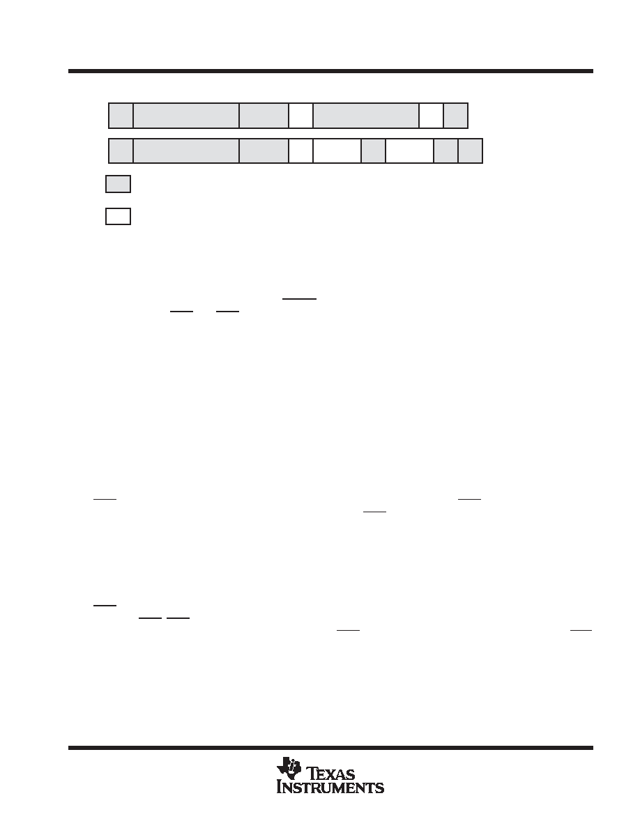
S
Slave Address
R
Data
A
S
Slave Address
W
Sub Address
A
P
Data
/A
P
From Transmitter
From Receiver
/
Not Acknowledge (SDA A High)
A
Acknowledge
S
Start Condition
P
Stop Condition
Figure 4. I2C Read Cycle
video port
The TFP6422/6424 Video Port is a low pin count, high-speed digital interface for a variety of digital video
formats. The video port consists of a 12-bit data bus (DATA[11:0]), horizontal timing signal (HSYNC), vertical
timing signal (VSYNC), blanking control (BLANK), clock signals (CLKOUT, CLKIN0 and CLKIN) and interrupt
request signals (INT0 and INT1). To reduce the pin count and the board space, a compact 12-bit pixel bus is
used. The bus operates in either single-pump or double-pump mode depending on the selection of the input
pixel format (FMT[2:0]). In single pump mode only the first edge of the CLKIN0/CLKIN1 differential clock pair
is used to sample the data, timing and blanking control signals. In double-pump mode, both edges of the clock
are used. With the double-pump mode high pixel transfer rates, up to 165 Mpixels/sec, can be achieved.
To ease the timing and EMI issues associated with a high pixel transfer rate, the signaling level of the signals
in Video Port is scalable. The input signals in video port are scalable by adjusting the voltage on the VREF pin
to VDDQ/2. Similarly, the output signals are scalable by adjusting the voltage on the VDDQ pin to VDDQ, where
VDDQ is the desirable full-swing voltage for the video port I/O signals. The differential CLKIN pair provides more
robust and reliable sampling for the pixel data and control signals, alleviating tight setup and hold time
requirements for high pixel transfer rates. Although differential clocking is the recommended clocking scheme,
it is possible to use single-end clocking with reduced timing margin, which may be significant with high clock
rates. When single-end clocking is used, CLKIN0 must be connected to the clock and CLKIN1 must be
connected to VDDQ/2.
INT1 and CLKOUT share the same pin. The function of the pin is defaulted to INT1 immediately after reset.
Reprogramming this may be done by writing to INTCKO bit. INT1 generates an interrupt to inform the host CPU
of events related to hot plug and power management. INT1# is open-drained and must be pulled up to VDDQ
with a 10K resistor. When programmed for CLKOUT function, CLKOUT pin outputs the clock generated by the
on-chip PLL. CLKOUT provides a reference clock which an external device, such as a graphics controller, may
to generate the CLKIN0 and CLKIN1 signals. CLKOUT signal is also tightly coupled to the progressive to
interlace conversion and overscan compensation functions. Refer to clock generation section for details for
clock generation and overscan compensation.
INT0 provides a dedicated interrupt for applications that need both CLKOUT signal and the interrupt signal.
Similar to INT1, INT0 is open–drained and normally a 10K pull-up resistor is needed to pull the signal to VDDQ.
TFP6422 and TFP6424 enters a special mode when INT0 is forced to low just before the deassertion of RST.
In this special mode, TFP6422 and TFP6424 is in simultaneous composite and S-video output mode, and
outputs an internally generated 100% color bar signal. No I2C programming is required to enable this feature.
This feature is very useful for initial system diagnostics during product development, but is not recommended
in the final product.
PRODUCT
PREVIEW
相關(guān)PDF資料 |
PDF描述 |
|---|---|
| TFP9431CPAP | SPECIALTY CONSUMER CIRCUIT, PQFP64 |
| TG355ENK-7916 | 8.15 MHz, LOW PASS FILTER |
| TH355BDI-4957 | 4.43 MHz, BAND PASS FILTER |
| TH355LDK-7915 | 8.15 MHz, LOW PASS FILTER |
| TH355LNK-4550 | 10 MHz, LOW PASS FILTER |
相關(guān)代理商/技術(shù)參數(shù) |
參數(shù)描述 |
|---|---|
| TFP70N06 | 制造商:TAK_CHEONG 制造商全稱:Tak Cheong Electronics (Holdings) Co.,Ltd 功能描述:N-Channel Power MOSFET 70A, 60V, 0.014Ω |
| TFP730 | 制造商:TAK_CHEONG 制造商全稱:Tak Cheong Electronics (Holdings) Co.,Ltd 功能描述:N-Channel Power MOSFET 5.5A, 400V, 0.95Ω |
| TFP740 | 制造商:TAK_CHEONG 制造商全稱:Tak Cheong Electronics (Holdings) Co.,Ltd 功能描述:N-Channel Power MOSFET 10A, 400V, 0.55Ω |
| TFP7433PZP | 制造商:Texas Instruments 功能描述: |
| TFP7445PZP-6 | 制造商:Texas Instruments 功能描述: |
發(fā)布緊急采購,3分鐘左右您將得到回復(fù)。