- 您現在的位置:買賣IC網 > PDF目錄373969 > AD9862 (Analog Devices, Inc.) Mixed-Signal Front-End (MxFE⑩) Processor for Broadband Communications PDF資料下載
參數資料
| 型號: | AD9862 |
| 廠商: | Analog Devices, Inc. |
| 英文描述: | Mixed-Signal Front-End (MxFE⑩) Processor for Broadband Communications |
| 中文描述: | 混合寬帶通信信號前端(MxFE⑩)處理器 |
| 文件頁數: | 27/32頁 |
| 文件大小: | 617K |
| 代理商: | AD9862 |
第1頁第2頁第3頁第4頁第5頁第6頁第7頁第8頁第9頁第10頁第11頁第12頁第13頁第14頁第15頁第16頁第17頁第18頁第19頁第20頁第21頁第22頁第23頁第24頁第25頁第26頁當前第27頁第28頁第29頁第30頁第31頁第32頁
REV. 0
AD9860/AD9862
–27–
Tx Path (Normal Operation)
The DAC update rate, the Tx input data rate, and the rate of
CLKOUT2 (clock used to latch Tx input data) are the parameters
of interest for the transmit path data. These parameters, in addition
to the output signal bandwidth, are related to CLKIN by the settings
of the ADC Div2, the DLL multiplier, the CLKOUT2 Div, the
two edges, and the interpolation registers.
The Tx data is timed relative to the CLKOUT2 pin (unless it is
retimed relative to CLKOUT1 by setting Tx Retime register) and
the input Tx data is latched on either each rising edge, each
falling edge or both edges (controlled through the Inverse Sample
and two edges registers). The timing diagrams for these cases
are shown in Figure 12.
The Dual Tx data is multiplexed onto a single bus so that fewer
digital bits are necessary to transfer data. Throughout this discus-
sion of Tx path timing, Tx digital processing options other than
interpolation are ignored because they do not change data timing;
Tx data timing reflects whether single or dual channel data is
latched into the AD9860/AD9862.
The rates of CLKOUT2 (and the input data rate) are related
to CLKIN by the DLL Multiplier Register, the setting of the
CLKOUT2 Divide Factor Register and the register ADC Div2.
These relationships are shown in Table II.
Table II. CLKOUT2 Timing Relative to CLKIN
for Normal Operation Mode
DLL
Mult
CLKOUT2
Div Factor
CLK DIV2
CLKOUT2
1
2
4
CLKIN
CLKIN/2
CLKIN/4
1
1
2
4
2 CLKIN
CLKIN
CLKIN/2
No Div
2
1
2
4
4 CLKIN
2 CLKIN
CLKIN
4
1
2
4
CLKIN/2
CLKIN/4
CLKIN/8
1
1
2
4
CLKIN
CLKIN/2
CLKIN/4
Div by 2
2
1
2
4
2 CLKIN
CLKIN
CLKIN/2
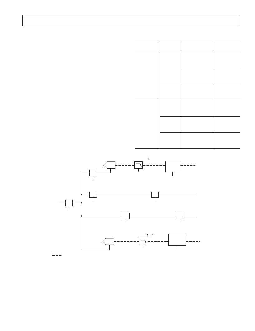
4
ADC
DATA MUX
AND
LATCH
DATA LATCH
AND
DEMUX
NO DECIMATION, 2
DECIMATE:
REG D6 B0
MUX OUT: REG D5 B0
Rx RETIME: REG D5 B3
2 DATA PATHS: REG D19 B4
Q/I ORDER: REG D18 B5
Tx RETIME: REG D18 B6
NO INTERP, 2, 4
INTERPOLATION:
REG D19 B0, 1
INV
NO INVERSION, INVERT
INV1: REG D25 B1
INV
DIV
1 , 1/2 , 1/4
NO INVERSION, INVERT
INV2: REG D25 B5
CLKOUT2 DIV FACTOR:
REG 25 B6, 7
DAC
CLKIN
Rx DATA
[0:23]
CLKOUT1
CLKOUT2
Tx DATA
[0:13]
DLL MULTIPLIER:
REG D24 B3, 4
DLL
1 , 2 , 4
DIV
1 , 1/2
CLKSEL
1 , 1/2
ADC DIV2:
REG D24 B5
DIV
CLOCK PATH
DATA PATH
Figure 13. Alternative Operation Timing Block Diagram
相關PDF資料 |
PDF描述 |
|---|---|
| AD9862BST | Mixed-Signal Front-End (MxFE⑩) Processor for Broadband Communications |
| AD9864 | IF Digitizing Subsystem |
| AD9864-EB | IF Digitizing Subsystem |
| AD9864BCPZ | IF Digitizing Subsystem |
| AD9864BCPZRL | IF Digitizing Subsystem |
相關代理商/技術參數 |
參數描述 |
|---|---|
| AD9862BST | 制造商:Analog Devices 功能描述:Mixed Signal Front End 128-Pin LQFP 制造商:Rochester Electronics LLC 功能描述:12B MIXED SIGNAL FRONT END MXFE PROCESSO - Tape and Reel |
| AD9862BSTRL | 制造商:Analog Devices 功能描述:Mixed Signal Front End 128-Pin LQFP T/R 制造商:Rochester Electronics LLC 功能描述:12B MIXED SIGNAL FRONT END MXFE PROCESSO - Tape and Reel |
| AD9862BSTZ | 功能描述:IC FRONT-END MIXED-SGNL 128-LQFP RoHS:是 類別:RF/IF 和 RFID >> RF 前端 (LNA + PA) 系列:- 產品培訓模塊:Lead (SnPb) Finish for COTS Obsolescence Mitigation Program 標準包裝:250 系列:- RF 型:GPS 頻率:1575.42MHz 特點:- 封裝/外殼:48-TQFP 裸露焊盤 供應商設備封裝:48-TQFP 裸露焊盤(7x7) 包裝:托盤 |
| AD9862BSTZRL | 功能描述:IC PROCESSOR FRONT END 128LQFP RoHS:是 類別:RF/IF 和 RFID >> RF 前端 (LNA + PA) 系列:- 產品培訓模塊:Lead (SnPb) Finish for COTS Obsolescence Mitigation Program 標準包裝:250 系列:- RF 型:GPS 頻率:1575.42MHz 特點:- 封裝/外殼:48-TQFP 裸露焊盤 供應商設備封裝:48-TQFP 裸露焊盤(7x7) 包裝:托盤 |
| AD9862-EB | 制造商:Analog Devices 功能描述: 制造商:Analog Devices 功能描述:MIXED SIGNAL FRONT END - Bulk |
發布緊急采購,3分鐘左右您將得到回復。