- 您現在的位置:買賣IC網 > PDF目錄374033 > ADSP-21266SKSTZ-2D (ANALOG DEVICES INC) SHARC Embedded Processor PDF資料下載
參數資料
| 型號: | ADSP-21266SKSTZ-2D |
| 廠商: | ANALOG DEVICES INC |
| 元件分類: | 數字信號處理 |
| 英文描述: | SHARC Embedded Processor |
| 中文描述: | 16-BIT, 66.67 MHz, OTHER DSP, PQFP144 |
| 封裝: | ROHS COMPLIANT, MS-026BFB, LQFP-144 |
| 文件頁數: | 37/44頁 |
| 文件大小: | 426K |
| 代理商: | ADSP-21266SKSTZ-2D |
第1頁第2頁第3頁第4頁第5頁第6頁第7頁第8頁第9頁第10頁第11頁第12頁第13頁第14頁第15頁第16頁第17頁第18頁第19頁第20頁第21頁第22頁第23頁第24頁第25頁第26頁第27頁第28頁第29頁第30頁第31頁第32頁第33頁第34頁第35頁第36頁當前第37頁第38頁第39頁第40頁第41頁第42頁第43頁第44頁
ADSP-21266
Rev. B
|
Page 37 of 44
|
May 2005
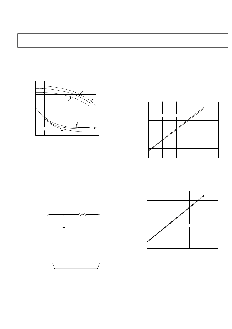
OUTPUT DRIVE CURRENTS
Figure 28
shows typical I-V characteristics for the output driv-
ers of the ADSP-21266. The curves represent the current drive
capability of the output drivers as a function of output voltage.
TEST CONDITIONS
The ac signal specifications (timing parameters) appear in
Table 11 on Page 19
through
Table 32 on Page 36
. These include
output disable time, output enable time, and capacitive loading.
Timing is measured on signals when they cross the 1.5 V level as
described in
Figure 30
. All delays (in nanoseconds) are mea-
sured between the point that the first signal reaches 1.5 V and
the point that the second signal reaches 1.5 V.
CAPACITIVE LOADING
Output delays and holds are based on standard capacitive loads:
30 pF on all pins (see
Figure 29
).
Figure 32
shows graphically
how output delays and holds vary with load capacitance (note
that this graph or derating does not apply to output disable
delays). The graphs of
Figure 31
,
Figure 32
, and
Figure 33
may
not be linear outside the ranges shown for Typical Output Delay
vs. Load Capacitance and Typical Output Rise Time (20%
–
80%,
V=Min) vs. Load Capacitance.
Figure 28. Typical Drive
Figure 29. Equivalent Device Loading for AC Measurements
(Includes All Fixtures)
Figure 30. Voltage Reference Levels for AC Measurements
SWEEP(VDDEXT) VOLTAGE (V)
–20
0
3.5
0.5
1
1.5
2
2.5
3
0
–40
–30
20
40
–10
S
VOL
3.11V, 125°C
3.3V, 25°C
3.47V, –45°C
VOH
30
10
3.11V, 125°C
3.3V, 25°C
3.47V, –45°C
1.5V
30pF
TO
OUTPUT
PIN
50
INPUT
OR
OUTPUT
1.5V
1.5V
Figure 31. Typical Output Rise Time
(20%
–
80%, V
DDEXT
= Max)
Figure 32. Typical Output Rise/Fall Time
(20%
–
80%, V
DDEXT
= Min)
LOAD CAPACITANCE (pF)
8
0
0
100
250
12
4
2
10
6
R
200
150
50
FALL
y = 0.0467x + 1.6323
y = 0.045x + 1.524
RISE
LOAD CAPACITANCE (pF)
12
0
50
100
150
200
250
10
8
6
4
R
2
0
RISE
FALL
y = 0.049x + 1.5105
y = 0.0482x + 1.4604
相關PDF資料 |
PDF描述 |
|---|---|
| ADSP-21363 | SHARC Processor |
| ADSP-21363SBBC-ENG | SHARC Processor |
| ADSP-21363SBBCZENG | SHARC Processor |
| ADSP-21364 | SHARC Processor |
| ADSP-21364SBBC-ENG | SHARC Processor |
相關代理商/技術參數 |
參數描述 |
|---|---|
| ADSP-21267 | 制造商:AD 制造商全稱:Analog Devices 功能描述:Preliminary Technical Data |
| ADSP-21267SKBCZ-X | 制造商:AD 制造商全稱:Analog Devices 功能描述:Preliminary Technical Data |
| ADSP-21267SKSTZ-X | 制造商:AD 制造商全稱:Analog Devices 功能描述:Preliminary Technical Data |
| ADSP-21362 | 制造商:AD 制造商全稱:Analog Devices 功能描述:SHARC Processor |
| adsp-21362bbc-1aa | 制造商:Analog Devices 功能描述: |
發布緊急采購,3分鐘左右您將得到回復。