- 您現在的位置:買賣IC網 > Datasheet目錄45 > NCT7491RQR2G (ON Semiconductor)IC REMOTE THERMAL MONITOR 24QSOP Datasheet資料下載
參數資料
| 型號: | NCT7491RQR2G |
| 廠商: | ON Semiconductor |
| 文件頁數: | 11/80頁 |
| 文件大小: | 844K |
| 描述: | IC REMOTE THERMAL MONITOR 24QSOP |
| 標準包裝: | 2,500 |
| 系列: | * |
第1頁第2頁第3頁第4頁第5頁第6頁第7頁第8頁第9頁第10頁當前第11頁第12頁第13頁第14頁第15頁第16頁第17頁第18頁第19頁第20頁第21頁第22頁第23頁第24頁第25頁第26頁第27頁第28頁第29頁第30頁第31頁第32頁第33頁第34頁第35頁第36頁第37頁第38頁第39頁第40頁第41頁第42頁第43頁第44頁第45頁第46頁第47頁第48頁第49頁第50頁第51頁第52頁第53頁第54頁第55頁第56頁第57頁第58頁第59頁第60頁第61頁第62頁第63頁第64頁第65頁第66頁第67頁第68頁第69頁第70頁第71頁第72頁第73頁第74頁第75頁第76頁第77頁第78頁第79頁第80頁
NCT7491
http://onsemi.com
11
SMBus Slave Interface
Control of the NCT7491 is carried out using the serial
system management bus (SMBus). The NCT7491 is
connected to this bus as a slave device, under the control of
a master controller. The NCT7491 has a 7bit serial bus
address. When the device is powered up with the ADDREN
pin high, the NCT7491 has a default SMBus address of
0101110 or 0x2E. The read/write bit must be added to get the
8bit address.
If more than one NCT7491 is to be used in a system, each
additional NCT7491 is placed in address select mode by
strapping ADDREN low on powerup. The logic state of the
ADDRESS SELECT pin then determines the devices
SMBus address.
The device address is latched on the first valid SMBus
transaction, more precisely on the lowtohigh transition at
the beginning of the eighth SCL pulse, when the serial bus
address byte matches the selected slave address. Any
attempted changes in the address have no effect after this.
SMBus Addressing Options
Table 5. SETTING THE SMBUS ADDRESS
ADDREN
pin state
ADDRESS SELECT
pin state
Address
0
Low (10 kW to GND)
0101100 (0x2C)
0
High (10 kW pullup)
0101101 (0x2D)
1
Dont care
0101110 (0x2E)
Data is sent over the serial bus in sequences of nine clock
pulses: eight bits of data followed by an acknowledge bit
from the slave device. Transitions on the data line must
occur during the low period of the clock signal and remain
stable during the high period, because a lowtohigh
transition when the clock is high may be interpreted as a stop
signal. The number of data bytes that can be transmitted over
the serial bus in a single read or write operation is limited
only by what the master and slave devices can handle.
When all data bytes have been read or written, stop
conditions are established. In write mode, the master floats
the data line high after the 10th clock rising edge to assert a
stop condition. In read mode, the master device overrides the
acknowledge bit by floating the data line high during the low
period before the ninth clock pulse; this is known as No
acknowledge. The master takes the data line low during the
low period before the 10th clock rising edge, and then high
afetr the 10th clock rising edge to assert a stop condition.
In the NCT7491, write operations contain either one or
two bytes, and read operations contain one byte. To write
data to one of the device data registers or read data from it,
the address pointer register must be set so that the correct
data register is addressed. Then data can be written into that
register or read from it. The first byte of a write operation
always contains an address that is stored in the address
pointer register. If data is to be written to the device, the write
operation must contain a second data byte that is written to
the register selected by the address pointer register.
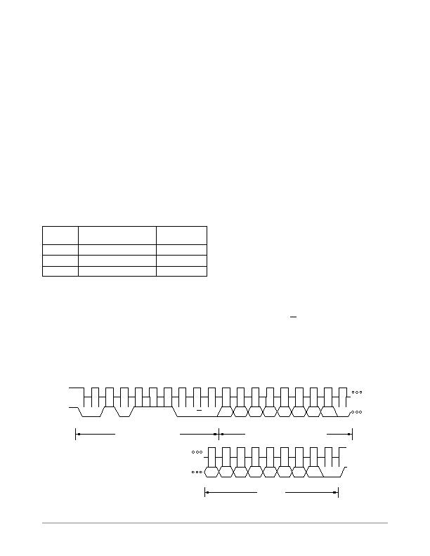
This write operation is shown in Figure 4. The device
address is sent over the bus, and then R/W
is set to 0. This
is followed by two data bytes. The first data byte is the
address of the internal data register to be written to, which
is stored in the address pointer register. The second data byte
is the data to be written to the internal data register.
When reading data from a register, there are two
possibilities:
" If the NCT7491 address pointer register value is
unknown or not the desired value, it must first be set to
the correct value before data can be read from the
desired data register. This is done by performing a write
to the NCT7491 as before, but only the data byte
containing the register address is sent because no data is
written to the register. This is shown in Figure 5.
A read operation is then performed consisting of the
serial bus address, R/W
bit set to 1, followed by the
data byte read from the data register. This is shown in
Figure 6.
" If the address pointer register is known to be already at
the desired address, data can be read from the
corresponding data register without first writing to the
address pointer register, as shown in Figure 6.
R/W
0
SCL
SDA
1
0
1
1
1
0
D7
D6
D5
D4
D3
D2
D1
D0
ACK. BY
ADT7490
START BY
MASTER
1
9
1
ACK. BY
ADT7490
9
D7
D6
D5
D4
D3
D2
D1
D0
ACK. BY
ADT7490
STOP BY
MASTER
1
9
SCL (CONTINUED)
SDA (CONTINUED)
FRAME 1
SERIAL BUS ADDRESS BYTE
FRAME 2
ADDRESS POINTER REGISTER BYTE
FRAME 3
DATA BYTE
Figure 4. Writing a Register Address to the Address Pointer Register, then Writing Data to the Selected Register
相關PDF資料 |
PDF描述 |
|---|---|
| NCT75MNR2G | IC SENSOR TEMP DGTL 8DFN |
| NCV8881PWR2G | IC REG TRPL BUCK/LINEAR 16SOIC |
| NE1617ADS,112 | IC TEMP MONITOR 16SSOP |
| NE1619DS,118 | IC TEMP MONITOR 16SSOP |
| NIS5112D1R2G | IC ELECTRONIC FUSE HOTSWAP 8SOIC |
相關代理商/技術參數 |
參數描述 |
|---|---|
| NCT75DMR2G | 功能描述:板上安裝溫度傳感器 2-Channel Digital Thermometer w/ Alarm RoHS:否 制造商:Omron Electronics 輸出類型:Digital 配置: 準確性:+/- 1.5 C, +/- 3 C 溫度閾值: 數字輸出 - 總線接口:2-Wire, I2C, SMBus 電源電壓-最大:5.5 V 電源電壓-最小:4.5 V 最大工作溫度:+ 50 C 最小工作溫度:0 C 關閉: 安裝風格: 封裝 / 箱體: 設備功能:Temperature and Humidity Sensor |
| NCT75DR2G | 功能描述:板上安裝溫度傳感器 2-Channel Digital Thermometer w/ Alarm RoHS:否 制造商:Omron Electronics 輸出類型:Digital 配置: 準確性:+/- 1.5 C, +/- 3 C 溫度閾值: 數字輸出 - 總線接口:2-Wire, I2C, SMBus 電源電壓-最大:5.5 V 電源電壓-最小:4.5 V 最大工作溫度:+ 50 C 最小工作溫度:0 C 關閉: 安裝風格: 封裝 / 箱體: 設備功能:Temperature and Humidity Sensor |
| NCT75MNR2G | 功能描述:板上安裝溫度傳感器 HAS2MONOJLCC84SPACE RoHS:否 制造商:Omron Electronics 輸出類型:Digital 配置: 準確性:+/- 1.5 C, +/- 3 C 溫度閾值: 數字輸出 - 總線接口:2-Wire, I2C, SMBus 電源電壓-最大:5.5 V 電源電壓-最小:4.5 V 最大工作溫度:+ 50 C 最小工作溫度:0 C 關閉: 安裝風格: 封裝 / 箱體: 設備功能:Temperature and Humidity Sensor |
| NCT7717U TR | 制造商:Nuvoton Technology Corp 功能描述:SMBUS INTERFACE TEMP. SENSOR W 制造商:Nuvoton Technology Corp 功能描述:IC SMBUS TEMP SENSOR 8MSOP |
| NCT7718W TR | 制造商:Nuvoton Technology Corp 功能描述:IC SMBUS TEMP SENSOR 8MSOP |
發布緊急采購,3分鐘左右您將得到回復。