- 您現在的位置:買賣IC網 > Datasheet目錄45 > NCT7491RQR2G (ON Semiconductor)IC REMOTE THERMAL MONITOR 24QSOP Datasheet資料下載
參數資料
| 型號: | NCT7491RQR2G |
| 廠商: | ON Semiconductor |
| 文件頁數: | 65/80頁 |
| 文件大小: | 844K |
| 描述: | IC REMOTE THERMAL MONITOR 24QSOP |
| 標準包裝: | 2,500 |
| 系列: | * |
第1頁第2頁第3頁第4頁第5頁第6頁第7頁第8頁第9頁第10頁第11頁第12頁第13頁第14頁第15頁第16頁第17頁第18頁第19頁第20頁第21頁第22頁第23頁第24頁第25頁第26頁第27頁第28頁第29頁第30頁第31頁第32頁第33頁第34頁第35頁第36頁第37頁第38頁第39頁第40頁第41頁第42頁第43頁第44頁第45頁第46頁第47頁第48頁第49頁第50頁第51頁第52頁第53頁第54頁第55頁第56頁第57頁第58頁第59頁第60頁第61頁第62頁第63頁第64頁當前第65頁第66頁第67頁第68頁第69頁第70頁第71頁第72頁第73頁第74頁第75頁第76頁第77頁第78頁第79頁第80頁
NCT7491
http://onsemi.com
65
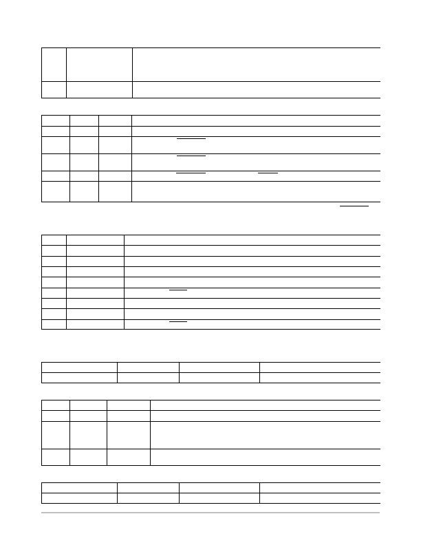
Table 97. REGISTER 0x81 Interrupt Status Register 4 (PowerOn Default = 0x00)
Bit
Description
R/W
Name
<6>
SMBCNT
R
Logic 1 indicates that the byte count returned by the SMBus Master Block Read is too low. If the
PCH temperature only is required then the returned byte count should be 2 or greater. If DIMM
temperatures are being read from the PCH then the returned byte count should be 9 or greater.
<7>
V
TT
R
A logic 1 indicates that the V
TT
high or low limit has been exceeded. This bit is cleared on a read
of the status register only if the error condition has subsided.
Table 98. REGISTER 0x82 Interrupt Mask Register 3 (PowerOn Default = 0x00)
Bit
Name
R/W
Description
<0>
PECI0
R/W
A logic 1 masks SMBALERT
assertions for outoflimit conditions on PECI0.
<1>
DATA
R/W
A logic 1 masks SMBALERT
assertions for PECI Data errors. This also disables the fan override
function for PECI errors.
<2>
COMM
R/W
A logic 1 masks SMBALERT
assertions for PECI communications errors. This also disables the
fan override function for PECI errors.
<3>
OVT
R/W
OVT = 1 masks SMBALERT
for over temperature THERM
conditions.
<6:4>
RES
R/W
Reserved
<7>
R
Reserved
NOTE: If the mask bits in register 0x82 are set it is also necessary to set the OOL mask bit in register 0x75 to ensure the SMBALERT
output is not asserted.
Table 99. REGISTER 0x83 Interrupt Mask Register 4 (PowerOn Default = 0x00)
Bit
Name
R/W
Description
<0>
PCC
R/W
Logic 1 masks ALERT
assertions for PECI completion codes.
<1>
TTS
R/W
Logic 1 masks assertions for THERM Timer status bit
<2>
GCOMM
R/W
Logic 1 masks the GCOMM PECI status bit
<3>
PECI1
R/W
A logic 1 masks ALERT
assertions for outoflimit conditions on PECI1.
<4>
PECI2
R/W
A logic 1 masks ALERT
assertions for outoflimit conditions on PECI2.
<5>
PECI3
R/W
A logic 1 masks ALERT
assertions for outoflimit conditions on PECI3.
<6>
SMBCNT
R/W
Logic 1 masks ALERT
assertions for incorrect byte count values returned by the Block Read command
<7>
V
TT
R/W
A logic 1 masks ALERT
assertions for outoflimit conditions on V
TT
.
NOTE: If the mask bits in register 0x83 are set it is also necessary to set the OOL mask bit in register 0x82 to ensure the SMBALERT
output is not asserted.
Table 100. V
TT
LOW LIMIT REGISTER
Register Address
R/W
Description
PowerOn Default
0x84
R/W
V
TT
Low Limit
0x00
Table 101. REGISTER 0x85 GPIO Config2 (PowerOn Default = 0x80)
Bit
Name
R/W
Description
<4:0>
Reserved
<5>
GPIO3
R/W
If GPIO3 is set to input, this bit reflects the state of the pin. If GPIO3 is configured as an
output, writing to this register asserts the output high or low depending on the polarity.
<6>
GPIO3 POL
R/W
GPIO3 polarity bit. Set to 0 for active low. Set to1 for active high.
<7>
GPIO3 DIR
R/W
GPIO3 direction bit. Set to 1 for GPIO3 to act as an input, set to 0 for GPIO3 to act as an
output, OOL must also be masked.
Table 102. V
TT
HIGH LIMIT REGISTER
Register Address
R/W
Description
PowerOn Default
0x86
R/W
V
TT
High Limit
0xFF
相關PDF資料 |
PDF描述 |
|---|---|
| NCT75MNR2G | IC SENSOR TEMP DGTL 8DFN |
| NCV8881PWR2G | IC REG TRPL BUCK/LINEAR 16SOIC |
| NE1617ADS,112 | IC TEMP MONITOR 16SSOP |
| NE1619DS,118 | IC TEMP MONITOR 16SSOP |
| NIS5112D1R2G | IC ELECTRONIC FUSE HOTSWAP 8SOIC |
相關代理商/技術參數 |
參數描述 |
|---|---|
| NCT75DMR2G | 功能描述:板上安裝溫度傳感器 2-Channel Digital Thermometer w/ Alarm RoHS:否 制造商:Omron Electronics 輸出類型:Digital 配置: 準確性:+/- 1.5 C, +/- 3 C 溫度閾值: 數字輸出 - 總線接口:2-Wire, I2C, SMBus 電源電壓-最大:5.5 V 電源電壓-最小:4.5 V 最大工作溫度:+ 50 C 最小工作溫度:0 C 關閉: 安裝風格: 封裝 / 箱體: 設備功能:Temperature and Humidity Sensor |
| NCT75DR2G | 功能描述:板上安裝溫度傳感器 2-Channel Digital Thermometer w/ Alarm RoHS:否 制造商:Omron Electronics 輸出類型:Digital 配置: 準確性:+/- 1.5 C, +/- 3 C 溫度閾值: 數字輸出 - 總線接口:2-Wire, I2C, SMBus 電源電壓-最大:5.5 V 電源電壓-最小:4.5 V 最大工作溫度:+ 50 C 最小工作溫度:0 C 關閉: 安裝風格: 封裝 / 箱體: 設備功能:Temperature and Humidity Sensor |
| NCT75MNR2G | 功能描述:板上安裝溫度傳感器 HAS2MONOJLCC84SPACE RoHS:否 制造商:Omron Electronics 輸出類型:Digital 配置: 準確性:+/- 1.5 C, +/- 3 C 溫度閾值: 數字輸出 - 總線接口:2-Wire, I2C, SMBus 電源電壓-最大:5.5 V 電源電壓-最小:4.5 V 最大工作溫度:+ 50 C 最小工作溫度:0 C 關閉: 安裝風格: 封裝 / 箱體: 設備功能:Temperature and Humidity Sensor |
| NCT7717U TR | 制造商:Nuvoton Technology Corp 功能描述:SMBUS INTERFACE TEMP. SENSOR W 制造商:Nuvoton Technology Corp 功能描述:IC SMBUS TEMP SENSOR 8MSOP |
| NCT7718W TR | 制造商:Nuvoton Technology Corp 功能描述:IC SMBUS TEMP SENSOR 8MSOP |
發布緊急采購,3分鐘左右您將得到回復。