- 您現(xiàn)在的位置:買賣IC網(wǎng) > Datasheet目錄45 > NCT7491RQR2G (ON Semiconductor)IC REMOTE THERMAL MONITOR 24QSOP Datasheet資料下載
參數(shù)資料
| 型號: | NCT7491RQR2G |
| 廠商: | ON Semiconductor |
| 文件頁數(shù): | 35/80頁 |
| 文件大小: | 844K |
| 描述: | IC REMOTE THERMAL MONITOR 24QSOP |
| 標(biāo)準(zhǔn)包裝: | 2,500 |
| 系列: | * |
第1頁第2頁第3頁第4頁第5頁第6頁第7頁第8頁第9頁第10頁第11頁第12頁第13頁第14頁第15頁第16頁第17頁第18頁第19頁第20頁第21頁第22頁第23頁第24頁第25頁第26頁第27頁第28頁第29頁第30頁第31頁第32頁第33頁第34頁當(dāng)前第35頁第36頁第37頁第38頁第39頁第40頁第41頁第42頁第43頁第44頁第45頁第46頁第47頁第48頁第49頁第50頁第51頁第52頁第53頁第54頁第55頁第56頁第57頁第58頁第59頁第60頁第61頁第62頁第63頁第64頁第65頁第66頁第67頁第68頁第69頁第70頁第71頁第72頁第73頁第74頁第75頁第76頁第77頁第78頁第79頁第80頁
NCT7491
http://onsemi.com
35
List of Status Registers
The complete list of status registers is given below along
with their associated mask registers. The definitions for the
status bits for each of the registers can be found in the
register tables at the end of this document. OOL bits in any
register do not require to be masked as they do not assert the
SMBALERT pin.
Table 29. STATUS REGISTERS
Status Bits
Status
Register
Address
Mask
Register
Address
Indicates status assertions in re-
gisters 0x41, 0x7E, 0xB6, 0xB7,
0xB8, 0xB9, 0xBA and 0x89.
0x12
Not
applicable
Voltage & Analog temperature
out of limit bits. OOL bit for re-
gister 0x42.
0x41
0x74
Voltage, Fans, Diode Faults.
OOL bit for register 0x43.
0x42
0x75
PECI0 out of limit, PECI COMM/
DATA error, THERM assertion,
DATA error code. OOL bit for re-
gister 0x81.
0x43
0x82
PECI completion code error,
THERM timer error, Generic
COMM error, PECI13 out of lim-
it bits, PCH byte count error, V
TT
out of limit bit.
0x81
0x83
Push register out of limit bits
0x7E
0x7F
SMBus Master NACK errors
0xB6
0xBC
SMBus Master PEC errors
0xB7
0xBD
SMBus Master Timeout errors
0xB8
0xBE
SMBus Master out of limit bits
0xB9
0xBF
SMBus Master Data Invalid errors
0xBA
0xC0
Voltage Monitoring
The NCT7491 has 5 external voltage measurement
channels. It can also measure its own supply voltage, V
CC
.
The NCT7491 can measure 5 V, 12 V, and 2.5 V supplies,
and the processor core voltage V
CCP
(0 V to 3 V input). The
2.5 V input can be used to monitor a chipset supply voltage
in computer systems. The V
CC
supply voltage measurement
is carried out through the V
CC
pin. The PECI V
TT
voltage
is also measured and is the dedicated reference voltage for
the PECI circuitry.
AnalogtoDigital Converter
All analog inputs are multiplexed into the onchip,
successive approximation, analogtodigital converter.
This has a resolution of 10 bits. The basic input range is 0 V
to 2 V, but the inputs have builtin attenuators to allow
measurement of 2.5 V, 3.3 V, 5 V, 12 V, and the processor
core voltage V
CCP
without any external components. To
allow the tolerance of these supply voltages, the ADC
produces an output of 3/4 full scale (768 dec or 300 hex) for
the nominal input voltage, and so has adequate headroom to
cope with overvoltages.
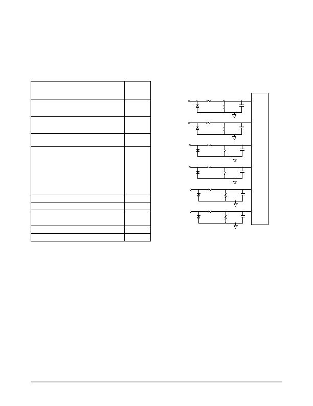
Voltage Input Circuitry
The internal structure for the analog inputs is shown in
Figure 24. The input circuit consists of an input protection
diode, an attenuator, plus a capacitor to form a firstorder
lowpass filter that gives input immunity to high frequency
noise. The attenuators can be disabled for the voltage
channels, except for the Vcc channel.
12 V
215.7 k
30.2 k
5 V
85.9 k
36.6 k
2.5 V
49.4 k
74 k
Vcc
66.7 k
55.8 k
Vccp
41.1 k
82.3 k
13.7 k
109.7 k
2.6 pF
Mux
Figure 24. Voltage Input Structures
V
TT
2.6 pF
2.6 pF
2.6 pF
2.6 pF
2.6 pF
Voltage Measurement Registers
" Reg. 0x1E, V
TT
Reading = 0x00 default
" Reg. 0x20, 2.5 V Reading = 0x00 default
" Reg. 0x21, V
CCP
Reading = 0x00 default
" Reg. 0x22, V
CC
Reading = 0x00 default
" Reg. 0x23, 5 V Reading = 0x00 default
" Reg. 0x24, 12 V Reading = 0x00 default
Extended Resolution Registers
Voltage measurements can be made with higher accuracy
using the extended resolution registers (0x1F, 0x76 and
0x77). Whenever the extended resolution registers are read,
the corresponding data in the voltage measurement registers
(0x1E, 0x20 to 0x24) is locked until their data is read. That
is, if extended resolution is required, the extended resolution
register must be read first immediately followed by
the appropriate voltage measurement register.
相關(guān)PDF資料 |
PDF描述 |
|---|---|
| NCT75MNR2G | IC SENSOR TEMP DGTL 8DFN |
| NCV8881PWR2G | IC REG TRPL BUCK/LINEAR 16SOIC |
| NE1617ADS,112 | IC TEMP MONITOR 16SSOP |
| NE1619DS,118 | IC TEMP MONITOR 16SSOP |
| NIS5112D1R2G | IC ELECTRONIC FUSE HOTSWAP 8SOIC |
相關(guān)代理商/技術(shù)參數(shù) |
參數(shù)描述 |
|---|---|
| NCT75DMR2G | 功能描述:板上安裝溫度傳感器 2-Channel Digital Thermometer w/ Alarm RoHS:否 制造商:Omron Electronics 輸出類型:Digital 配置: 準(zhǔn)確性:+/- 1.5 C, +/- 3 C 溫度閾值: 數(shù)字輸出 - 總線接口:2-Wire, I2C, SMBus 電源電壓-最大:5.5 V 電源電壓-最小:4.5 V 最大工作溫度:+ 50 C 最小工作溫度:0 C 關(guān)閉: 安裝風(fēng)格: 封裝 / 箱體: 設(shè)備功能:Temperature and Humidity Sensor |
| NCT75DR2G | 功能描述:板上安裝溫度傳感器 2-Channel Digital Thermometer w/ Alarm RoHS:否 制造商:Omron Electronics 輸出類型:Digital 配置: 準(zhǔn)確性:+/- 1.5 C, +/- 3 C 溫度閾值: 數(shù)字輸出 - 總線接口:2-Wire, I2C, SMBus 電源電壓-最大:5.5 V 電源電壓-最小:4.5 V 最大工作溫度:+ 50 C 最小工作溫度:0 C 關(guān)閉: 安裝風(fēng)格: 封裝 / 箱體: 設(shè)備功能:Temperature and Humidity Sensor |
| NCT75MNR2G | 功能描述:板上安裝溫度傳感器 HAS2MONOJLCC84SPACE RoHS:否 制造商:Omron Electronics 輸出類型:Digital 配置: 準(zhǔn)確性:+/- 1.5 C, +/- 3 C 溫度閾值: 數(shù)字輸出 - 總線接口:2-Wire, I2C, SMBus 電源電壓-最大:5.5 V 電源電壓-最小:4.5 V 最大工作溫度:+ 50 C 最小工作溫度:0 C 關(guān)閉: 安裝風(fēng)格: 封裝 / 箱體: 設(shè)備功能:Temperature and Humidity Sensor |
| NCT7717U TR | 制造商:Nuvoton Technology Corp 功能描述:SMBUS INTERFACE TEMP. SENSOR W 制造商:Nuvoton Technology Corp 功能描述:IC SMBUS TEMP SENSOR 8MSOP |
| NCT7718W TR | 制造商:Nuvoton Technology Corp 功能描述:IC SMBUS TEMP SENSOR 8MSOP |
發(fā)布緊急采購,3分鐘左右您將得到回復(fù)。