- 您現在的位置:買賣IC網 > PDF目錄373973 > AD9992BBCZRL (ANALOG DEVICES INC) 12-Bit CCD Signal Processor with Precision Timing Generator PDF資料下載
參數資料
| 型號: | AD9992BBCZRL |
| 廠商: | ANALOG DEVICES INC |
| 元件分類: | 消費家電 |
| 英文描述: | 12-Bit CCD Signal Processor with Precision Timing Generator |
| 中文描述: | SPECIALTY CONSUMER CIRCUIT, PBGA105 |
| 封裝: | 8 X 8 MM, 0.65 MM PITCH, ROHS COMPLIANT, MO-225, CSPBGA-105 |
| 文件頁數: | 24/92頁 |
| 文件大小: | 718K |
| 代理商: | AD9992BBCZRL |
第1頁第2頁第3頁第4頁第5頁第6頁第7頁第8頁第9頁第10頁第11頁第12頁第13頁第14頁第15頁第16頁第17頁第18頁第19頁第20頁第21頁第22頁第23頁當前第24頁第25頁第26頁第27頁第28頁第29頁第30頁第31頁第32頁第33頁第34頁第35頁第36頁第37頁第38頁第39頁第40頁第41頁第42頁第43頁第44頁第45頁第46頁第47頁第48頁第49頁第50頁第51頁第52頁第53頁第54頁第55頁第56頁第57頁第58頁第59頁第60頁第61頁第62頁第63頁第64頁第65頁第66頁第67頁第68頁第69頁第70頁第71頁第72頁第73頁第74頁第75頁第76頁第77頁第78頁第79頁第80頁第81頁第82頁第83頁第84頁第85頁第86頁第87頁第88頁第89頁第90頁第91頁第92頁
AD9992
HBLK Mode 2 Operation
HBLK Mode 2 allows more advanced HBLK pattern operation.
If multiple areas of HCLK pulses that are unevenly spaced apart
from one another are needed, HBLK Mode 2 can be used. Using
a separate set of registers, HBLK Mode 2 can divide the HBLK
region into up to six repeat areas (see Table 10). As shown in
Figure 29, each repeat area shares a common group of toggle
positions, HBLKSTARTA, HBLKSTARTB, and HBLKSTARTC.
However, the number of toggles following each start position
can be unique in each repeat area by using the RAH1REP and
RAH2REP registers. As shown in Figure 28, setting the
RAH1REPA/RAH1REPB/RAH1REPC or RAH2REPA/
RAH2REPB/RAH2REPC registers to 0 masks HCLK groups
from appearing in a particular repeat area. Figure 29 shows only
two repeat areas being used, although six are available. It is possible
to program a separate number of repeat area repetitions for H1
and H2, but generally the same value is used for both H1 and
H2. Figure 29 shows an example of RA0H1REPA/RA0H1REPB/
RA0H1REPC = RA0H2REPA/RA0H2REPB/RA0H2REPC =
RA1H1REPA/RA1H1REPB/RA1H1REPC = RA1H2REPA/
RA1H2REPB/RA1H2REPC = 2.
Rev. 0 | Page 24 of 92
Furthermore, HBLK Mode 2 allows a different HBLK pattern
on even and odd lines. The HBLKSTARTA, HBLKSTARTB, and
HBLKSTARTC registers, as well as the RAH1REPA/RAH1REPB/
RAH1REPC and RAH2REPA/RAH2REPB/RAH2REPC registers,
define operation for the even lines. For separate control of the
odd lines, the HBLKALT_PAT registers specify up to six repeat
areas on the odd lines by reordering the repeat areas used for the
even lines. New patterns are not available, but the order of the
previously defined repeat areas on the even lines can be changed
for the odd lines to accommodate advanced CCD operation.
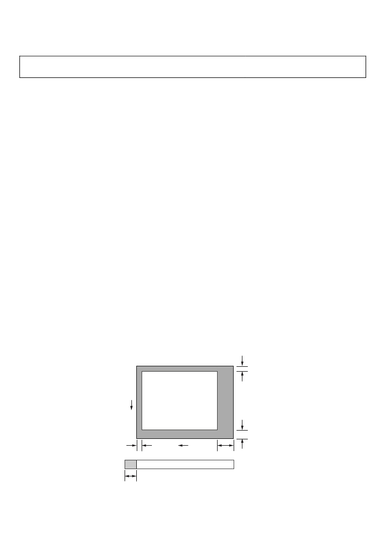
HORIZONTAL TIMING SEQUENCE EXAMPLE
Figure 30 shows an example CCD layout. The horizontal
register contains 28 dummy pixels, which occur on each line
clocked from the CCD. In the vertical direction, there are
10 optical black (OB) lines at the front of the readout and two at
the back of the readout. The horizontal direction has four OB
pixels in the front and 48 in the back.
Figure 31 shows the basic sequence layout to be used during the
effective pixel readout. The 48 OB pixels at the end of each line
are used for the CLPOB signals. PBLK is optional and is often
used to blank the digital outputs during the HBLK time. HBLK
is used during the vertical shift interval.
Because PBLK is used to isolate the CDS input (see the Analog
Preblanking section), the PBLK signal should not be used
during CLPOB operation. The change in the offset behavior
that occurs during PBLK impacts the accuracy of the CLPOB
circuitry.
The HBLK, CLPOB, and PBLK parameters are programmed in
the V-sequence registers. More elaborate clamping schemes,
such as adding in a separate sequence to clamp in the entire
shield OB lines, can be used. This requires configuring a
separate V-sequence for clocking out the OB lines.
The CLPMASK registers are also useful for disabling the
CLPOB on a few lines without affecting the setup of the
clamping sequences. It is important that CLPOB be used only
during valid OB pixels. During other portions on the frame
timing, such as vertical blanking or SG line timing, the CCD
does not output valid OB pixels. Any CLPOB pulse that occurs
during this time causes errors in clamping operation and
changes in the black level of the image.
HORIZONTAL CCD REGISTER
EFFECTIVE IMAGEAREA
28 DUMMY PIXELS
48 OB PIXELS
4 OB PIXELS
10 VERTICAL
OB LINES
2 VERTICAL
OB LINES
V
H
0
Figure 30. Example CCD Configuration
相關PDF資料 |
PDF描述 |
|---|---|
| AD9995KCP | 12-Bit CCD Signal Processor with Precision Timing ⑩ Generator |
| AD9995KCPRL | 12-Bit CCD Signal Processor with Precision Timing ⑩ Generator |
| AD9995 | 12-Bit CCD Signal Processor with Precision Timing ⑩ Generator |
| ADA4000-2ARMZ-RL | Low Cost, Precision JFET Input Operational Amplifiers |
| ADA4000-1 | Low Cost, Precision JFET Input Operational Amplifiers |
相關代理商/技術參數 |
參數描述 |
|---|---|
| AD9993BBCZ | 功能描述:IC MIXED-SIGNAL FRONT END 196BGA 制造商:analog devices inc. 系列:- 包裝:托盤 零件狀態:在售 類型:ADC,DAC 輸入類型:LVDS 輸出類型:LVDS 接口:SPI 電流 - 電源:- 工作溫度:- 安裝類型:表面貼裝 封裝/外殼:196-LFBGA,CSPBGA 供應商器件封裝:196-CSPBGA(12x12) 標準包裝:1 |
| AD9993BBCZRL | 功能描述:IC MIXED-SIGNAL FRONT END 196BGA 制造商:analog devices inc. 系列:- 包裝:帶卷(TR) 零件狀態:在售 類型:ADC,DAC 輸入類型:LVDS 輸出類型:LVDS 接口:SPI 電流 - 電源:- 工作溫度:- 安裝類型:表面貼裝 封裝/外殼:196-LFBGA,CSPBGA 供應商器件封裝:196-CSPBGA(12x12) 標準包裝:1,500 |
| AD9993-EBZ | 功能描述:EVAL BOARD MXFE AD9993 制造商:analog devices inc. 系列:* 零件狀態:在售 標準包裝:1 |
| AD9994 | 制造商:AD 制造商全稱:Analog Devices 功能描述:12-Bit CCD Signal Processor with Precision Timing Generator |
| AD9994BCP | 制造商:Analog Devices 功能描述:AFE GEN PURPOSE 12-BIT 64LFCSP - Bulk |
發布緊急采購,3分鐘左右您將得到回復。