- 您現(xiàn)在的位置:買賣IC網(wǎng) > PDF目錄373970 > AD9910 (Analog Devices, Inc.) 1 GSPS, 14-Bit, 3.3 V CMOS Direct Digital Synthesizer PDF資料下載
參數(shù)資料
| 型號: | AD9910 |
| 廠商: | Analog Devices, Inc. |
| 元件分類: | XO, clock |
| 英文描述: | 1 GSPS, 14-Bit, 3.3 V CMOS Direct Digital Synthesizer |
| 中文描述: | 1 GSPS的,14位,3.3伏的CMOS直接數(shù)字頻率合成 |
| 文件頁數(shù): | 17/60頁 |
| 文件大小: | 764K |
| 代理商: | AD9910 |
第1頁第2頁第3頁第4頁第5頁第6頁第7頁第8頁第9頁第10頁第11頁第12頁第13頁第14頁第15頁第16頁當(dāng)前第17頁第18頁第19頁第20頁第21頁第22頁第23頁第24頁第25頁第26頁第27頁第28頁第29頁第30頁第31頁第32頁第33頁第34頁第35頁第36頁第37頁第38頁第39頁第40頁第41頁第42頁第43頁第44頁第45頁第46頁第47頁第48頁第49頁第50頁第51頁第52頁第53頁第54頁第55頁第56頁第57頁第58頁第59頁第60頁
AD9910
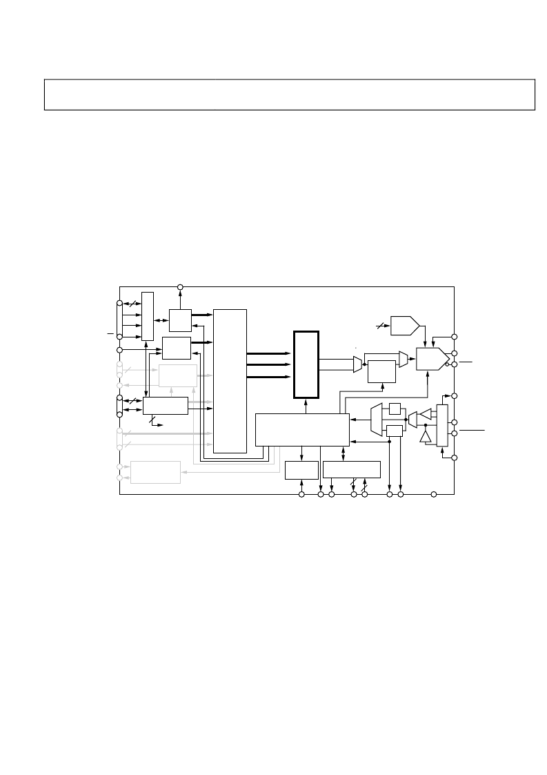
RAM MODULATION MODE
The RAM modulation mode (see Figure 23) is activated via the
RAM enable bit and assertion of the I/O_UPDATE pin (or a
profile change). In this mode, the modulated DDS signal
control parameters are supplied directly from RAM.
Rev. 0 | Page 17 of 60
The RAM consists of 32-bit words and is 1024 words deep.
Coupled with a sophisticated internal state machine, the RAM
provides a very flexible method for generating arbitrary, time
dependent waveforms. A programmable timer controls the rate
at which words are extracted from the RAM for delivery to the
DDS. Thus, the programmable timer establishes a sample rate at
which 32-bit samples are supplied to the DDS.
The selection of the specific DDS signal control parameters that
serve as the destination for the RAM samples is also programmable
through eight independent RAM profile registers. Select a par-
ticular profile using the three external profile pins (PROFILE<2:0>).
A change in the state of the profile pins with the next rising
edge on SYNC_CLK activates the selected RAM profile.
In RAM modulation mode, the ability to generate a time
dependent amplitude, phase, or frequency signal enables
modulation of any one of the parameters controlling the DDS
carrier signal. Furthermore, a polar modulation format is
available that partitions each RAM sample into a magnitude
and phase component; 16 bits allocated to phase and 14 bits
allocated to magnitude.
0
16
PARALLEL
INPUT
PDCLK
SCLK
SDIO
I/O_RESET
PROFILE
I/O_UPDATE
RAM
POWER
DOWN
CONTROL
E
DAC_RSET
IOUT
IOUT
CS
TxENABLE
DAC FSC
OSK
A
θ
INVERSE
SINC
FILTER
CLOCK
AMPLITUDE (A)
FREQUENCY (
ω
)
PHASE (
θ
)
DIGITAL
RAMP
GENERATOR
8
DAC FSC
8
2
2
MULTICHIP
SYNCHRONIZATION
SYSCLK
PLL
÷2
C
REF_CLK
REF_CLK
REFCLK_OUT
XTAL_SEL
PARALLEL DATA
TIMING AND
CONTROL
S
2
AD9910
PROGRAMMING
REGISTERS
OUTPUT
SHIFT
KEYING
DATA
ROUTE
AND
PARTITION
CONTROL
3
INTERNAL CLOCK TIMING
AND CONTROL
ω
Acos (
ω
t+
θ
)
Asin (
ω
t+
θ
)
S
S
S
P
P
M
2
2
DDS
AUX
DAC
8-BIT
DAC
14-BIT
RAM_SWP_OVR
DRCTL
DRHOLD
DROVER
S
Figure 23. RAM Modulation Mode
相關(guān)PDF資料 |
PDF描述 |
|---|---|
| AD9910_07 | 1 GSPS, 14-Bit, 3.3 V CMOS Direct Digital Synthesizer |
| AD9910BSVZ | 1 GSPS, 14-Bit, 3.3 V CMOS Direct Digital Synthesizer |
| AD9910BSVZ-REEL | 1 GSPS, 14-Bit, 3.3 V CMOS Direct Digital Synthesizer |
| AD9912 | 1 GSPS Direct Digital Synthesizer w/ 14-bit DAC |
| AD9913 | Low Power 250 MSPS 10-Bit DAC 1.8 V CMOS Direct Digital Synthesizer |
相關(guān)代理商/技術(shù)參數(shù) |
參數(shù)描述 |
|---|---|
| AD9910/PCBZ | 功能描述:數(shù)據(jù)轉(zhuǎn)換 IC 開發(fā)工具 1GSPS 14 bit DDS w/ parallel input port RoHS:否 制造商:Texas Instruments 產(chǎn)品:Demonstration Kits 類型:ADC 工具用于評估:ADS130E08 接口類型:SPI 工作電源電壓:- 6 V to + 6 V |
| AD9910_07 | 制造商:AD 制造商全稱:Analog Devices 功能描述:1 GSPS, 14-Bit, 3.3 V CMOS Direct Digital Synthesizer |
| AD9910BSVZ | 功能描述:IC DDS 1GSPS 14BIT PAR 100TQFP RoHS:是 類別:集成電路 (IC) >> 接口 - 直接數(shù)字合成 (DDS) 系列:- 產(chǎn)品變化通告:Product Discontinuance 27/Oct/2011 標(biāo)準(zhǔn)包裝:2,500 系列:- 分辨率(位):10 b 主 fclk:25MHz 調(diào)節(jié)字寬(位):32 b 電源電壓:2.97 V ~ 5.5 V 工作溫度:-40°C ~ 85°C 安裝類型:表面貼裝 封裝/外殼:16-TSSOP(0.173",4.40mm 寬) 供應(yīng)商設(shè)備封裝:16-TSSOP 包裝:帶卷 (TR) |
| AD9910BSVZ | 制造商:Analog Devices 功能描述:IC DDS 1GHZ TQFP-100 制造商:Analog Devices 功能描述:IC, DDS, 1GHZ, TQFP-100 |
| AD9910BSVZ-REEL | 功能描述:IC DDS 1GSPS 14BIT PAR 100TQFP RoHS:是 類別:集成電路 (IC) >> 接口 - 直接數(shù)字合成 (DDS) 系列:- 產(chǎn)品變化通告:Product Discontinuance 27/Oct/2011 標(biāo)準(zhǔn)包裝:2,500 系列:- 分辨率(位):10 b 主 fclk:25MHz 調(diào)節(jié)字寬(位):32 b 電源電壓:2.97 V ~ 5.5 V 工作溫度:-40°C ~ 85°C 安裝類型:表面貼裝 封裝/外殼:16-TSSOP(0.173",4.40mm 寬) 供應(yīng)商設(shè)備封裝:16-TSSOP 包裝:帶卷 (TR) |
發(fā)布緊急采購,3分鐘左右您將得到回復(fù)。