- 您現在的位置:買賣IC網 > PDF目錄373970 > AD9910 (Analog Devices, Inc.) 1 GSPS, 14-Bit, 3.3 V CMOS Direct Digital Synthesizer PDF資料下載
參數資料
| 型號: | AD9910 |
| 廠商: | Analog Devices, Inc. |
| 元件分類: | XO, clock |
| 英文描述: | 1 GSPS, 14-Bit, 3.3 V CMOS Direct Digital Synthesizer |
| 中文描述: | 1 GSPS的,14位,3.3伏的CMOS直接數字頻率合成 |
| 文件頁數: | 38/60頁 |
| 文件大小: | 764K |
| 代理商: | AD9910 |
第1頁第2頁第3頁第4頁第5頁第6頁第7頁第8頁第9頁第10頁第11頁第12頁第13頁第14頁第15頁第16頁第17頁第18頁第19頁第20頁第21頁第22頁第23頁第24頁第25頁第26頁第27頁第28頁第29頁第30頁第31頁第32頁第33頁第34頁第35頁第36頁第37頁當前第38頁第39頁第40頁第41頁第42頁第43頁第44頁第45頁第46頁第47頁第48頁第49頁第50頁第51頁第52頁第53頁第54頁第55頁第56頁第57頁第58頁第59頁第60頁
AD9910
Rev. 0 | Page 38 of 60
0
WAVEFORM START ADDRESS
WAVEFORM END ADDRESS
1
PROFILE0
RAM ADRESS
RAM_SWP_OVER
I/O_UPDATE
1
2
3
4
5
6
7
8
Δ
t
Δ
t
M DDS CLOCK CYCLES
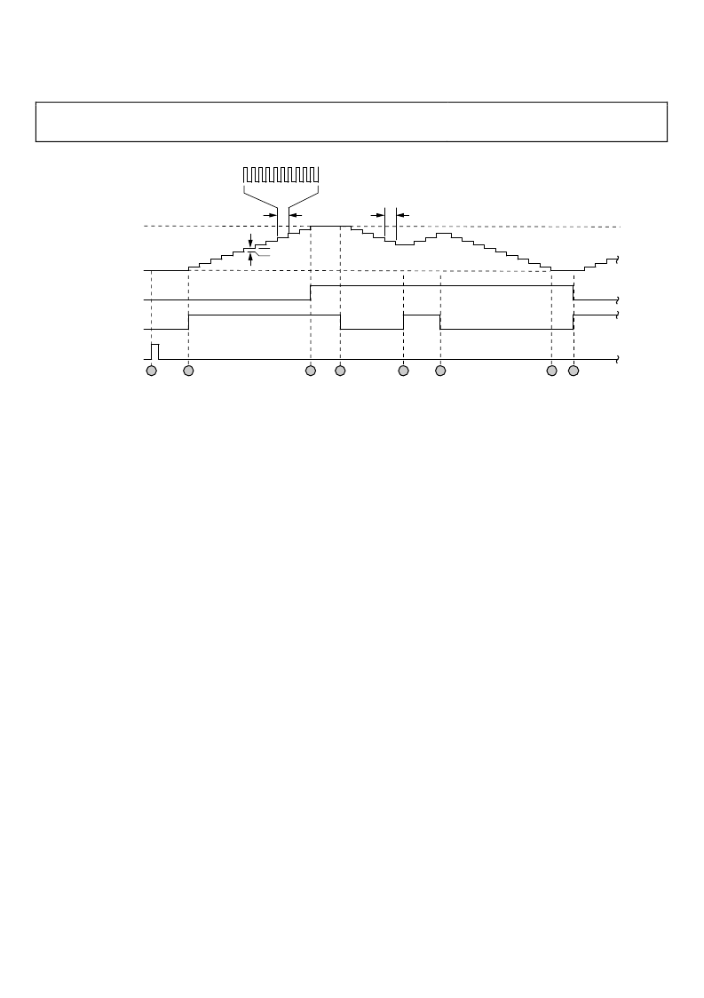
Figure 46. Bidirectional Ramp Timing Diagram
If the PROFILE0 pin changes states before the state machine
reaches the programmed start or end address, the internal timer
is restarted and the direction of the address counter is reversed.
Figure 46 is a graphic representation of the bidirectional ramp
mode. It shows the action of the state machine in response to
the PROFILE0 pin, and the response of the RAM_SWP_OVR pin.
The RAM_SWP_OVR pin switches to Logic 1 when the state
machine reaches the waveform end address. It remains Logic 1
until the state machine reaches the waveform start address and
the PROFILE0 pin transitions from Logic 0 to Logic 1.
The circled numbers in Figure 46 indicate specific events as
follows:
Event 1—An I/O update or profile change activates the RAM
bidirectional ramp mode. The state machine initializes to the
waveform start address and the RAM_SWP_OVR pin is set to
Logic 0.
Event 2—PROFILE0 pin switches to Logic 1. The state machine
begins incrementing the RAM address counter.
Event 3—PROFILE0 pin remains at Logic 1 long enough for
the state machine to reach the waveform end address. The
RAM_SWP_OVR pin switches to Logic 1 accordingly.
Event 4—PROFILE0 pin switches to Logic 0. The state
machine begins decrementing the RAM address counter.
The RAM_SWP_OVR pin remains at Logic 1.
Event 5—PROFILE0 pin switches to Logic 1. The state machine
resets its internal timer and reverses the direction of the RAM
address counter (that is, it starts to increment). No change of
the RAM_SWP_OVR state because the waveform start address
has not yet been reached.
Event 6—PROFILE0 pin switches to Logic 0. The state machine
resets its internal timer and again reverses the direction of the RAM
address counter. The RAM_SWP_OVR state does not change.
Event 7—PROFILE0 pin remains at Logic 0 long enough for the
state machine to reach the waveform start address. There is no
change in the RAM_SWP_OVR state.
Event 8—PROFILE0 pin switches to Logic 1. The state machine
resets its internal timer and begins incrementing the RAM
address counter. The RAM_SWP_OVR pin switches to Logic 0
because both the waveform start address was reached and the
PROFILE0 pin transitioned from Logic 0 to Logic 1.
RAM Continuous Bidirectional Ramp Mode
In continuous bidirectional ramp mode, upon assertion of an
I/O update or a change of profile, the RAM begins operating as
a waveform generator using the parameters programmed into
the RAM profile designated by the profile pins. Data is extracted
from RAM over the specified address range and at the specified
rate contained in the waveform start address, waveform end
address, and address ramp rate values of the selected RAM
profile. The data is delivered to the specified DDS signal control
parameter(s) based on the RAM playback destination bits. The
no-dwell high bit is ignored in this mode.
With the continuous bidirectional ramp mode activated via an
I/O update or profile change, the internal state machine begins
extracting data from the RAM at the waveform start address
and incrementing the address counter until it reaches the
waveform end address. At this point, the state machine
automatically reverses the direction of the address counter and
begins decrementing through the address range. Whenever one
of the terminal addresses is reached, the state machine reverses
the address counter; the process continues indefinitely.
相關PDF資料 |
PDF描述 |
|---|---|
| AD9910_07 | 1 GSPS, 14-Bit, 3.3 V CMOS Direct Digital Synthesizer |
| AD9910BSVZ | 1 GSPS, 14-Bit, 3.3 V CMOS Direct Digital Synthesizer |
| AD9910BSVZ-REEL | 1 GSPS, 14-Bit, 3.3 V CMOS Direct Digital Synthesizer |
| AD9912 | 1 GSPS Direct Digital Synthesizer w/ 14-bit DAC |
| AD9913 | Low Power 250 MSPS 10-Bit DAC 1.8 V CMOS Direct Digital Synthesizer |
相關代理商/技術參數 |
參數描述 |
|---|---|
| AD9910/PCBZ | 功能描述:數據轉換 IC 開發工具 1GSPS 14 bit DDS w/ parallel input port RoHS:否 制造商:Texas Instruments 產品:Demonstration Kits 類型:ADC 工具用于評估:ADS130E08 接口類型:SPI 工作電源電壓:- 6 V to + 6 V |
| AD9910_07 | 制造商:AD 制造商全稱:Analog Devices 功能描述:1 GSPS, 14-Bit, 3.3 V CMOS Direct Digital Synthesizer |
| AD9910BSVZ | 功能描述:IC DDS 1GSPS 14BIT PAR 100TQFP RoHS:是 類別:集成電路 (IC) >> 接口 - 直接數字合成 (DDS) 系列:- 產品變化通告:Product Discontinuance 27/Oct/2011 標準包裝:2,500 系列:- 分辨率(位):10 b 主 fclk:25MHz 調節字寬(位):32 b 電源電壓:2.97 V ~ 5.5 V 工作溫度:-40°C ~ 85°C 安裝類型:表面貼裝 封裝/外殼:16-TSSOP(0.173",4.40mm 寬) 供應商設備封裝:16-TSSOP 包裝:帶卷 (TR) |
| AD9910BSVZ | 制造商:Analog Devices 功能描述:IC DDS 1GHZ TQFP-100 制造商:Analog Devices 功能描述:IC, DDS, 1GHZ, TQFP-100 |
| AD9910BSVZ-REEL | 功能描述:IC DDS 1GSPS 14BIT PAR 100TQFP RoHS:是 類別:集成電路 (IC) >> 接口 - 直接數字合成 (DDS) 系列:- 產品變化通告:Product Discontinuance 27/Oct/2011 標準包裝:2,500 系列:- 分辨率(位):10 b 主 fclk:25MHz 調節字寬(位):32 b 電源電壓:2.97 V ~ 5.5 V 工作溫度:-40°C ~ 85°C 安裝類型:表面貼裝 封裝/外殼:16-TSSOP(0.173",4.40mm 寬) 供應商設備封裝:16-TSSOP 包裝:帶卷 (TR) |
發布緊急采購,3分鐘左右您將得到回復。