- 您現在的位置:買賣IC網 > PDF目錄373970 > AD9910 (Analog Devices, Inc.) 1 GSPS, 14-Bit, 3.3 V CMOS Direct Digital Synthesizer PDF資料下載
參數資料
| 型號: | AD9910 |
| 廠商: | Analog Devices, Inc. |
| 元件分類: | XO, clock |
| 英文描述: | 1 GSPS, 14-Bit, 3.3 V CMOS Direct Digital Synthesizer |
| 中文描述: | 1 GSPS的,14位,3.3伏的CMOS直接數字頻率合成 |
| 文件頁數: | 27/60頁 |
| 文件大小: | 764K |
| 代理商: | AD9910 |
第1頁第2頁第3頁第4頁第5頁第6頁第7頁第8頁第9頁第10頁第11頁第12頁第13頁第14頁第15頁第16頁第17頁第18頁第19頁第20頁第21頁第22頁第23頁第24頁第25頁第26頁當前第27頁第28頁第29頁第30頁第31頁第32頁第33頁第34頁第35頁第36頁第37頁第38頁第39頁第40頁第41頁第42頁第43頁第44頁第45頁第46頁第47頁第48頁第49頁第50頁第51頁第52頁第53頁第54頁第55頁第56頁第57頁第58頁第59頁第60頁
AD9910
The step interval is controlled by a 16-bit programmable timer
that is clocked at a rate of f
SYSCLK
. The period of the timer sets
the time interval between amplitude steps. The step time interval
(Δt) is given by
M
t
Δ
=
Rev. 0 | Page 27 of 60
SYSCLK
f
4
where
M
is the 16-bit number stored in the amplitude ramp rate
(ARR) portion of the ASF register. For example, if f
SYSCLK
=
750 MHz and M = 23218 (0x5AB2), then Δt ≈
123.8293 μs.
The output of the OSK function is a 14-bit unsigned data bus
that controls the amplitude parameter of the DDS (as long as
the OSK enable bit is set). When the OSK pin is set, the OSK
output value starts at 0 (zero) and increments by the pro-
grammed amplitude step size until it reaches the programmed
maximum amplitude value. When the OSK pin is cleared, the
OSK output starts at its present value and decrements by the
programmed amplitude step size until it reaches 0 (zero).
The OSK output does not necessarily attain the maximum
amplitude value if the OSK pin is switched to Logic 0 before the
maximum value is reached. Nor does the OSK output necessarily
reach a value of zero if the OSK pin is switched to Logic 1
before the zero value is reached.
The OSK output is initialized to 0 (zero) at power-up and reset
whenever the OSK enable bit or the select auto OSK bit is cleared.
The amplitude step size of the OSK output is set by the amplitude
step size bits in the ASF register according to Table 10. The step
size refers to the LSB weight of the 14-bit OSK output. Regardless
of the programmed step size, the OSK output does not exceed
the maximum amplitude value programmed into the ASF
register.
Table 10. OSK Amplitude Step Size
ASF<1:0>
00
01
10
11
Amplitude Step Size
1
2
4
8
As mentioned previously, a 16-bit programmable timer controls the
step interval. Normally, this timer is loaded with the programmed
timing value whenever the timer expires, initiating a new timing
cycle. However, there are three events that can cause reloading of
the timer to have its timing value reloaded prior to the timer
expiring. One such event is when the select auto
OSK bit is
transitioned from cleared to set followed by an I/O update. A
second such event is a change of state in the OSK pin. The third is
dependent on the status of the Load ARR @ I/O Update bit. If this
bit is cleared, then no action occurs, otherwise, when the
I/O_UPDATE pin is asserted (or a profile change occurs), the timer
is reset to its initial starting point.
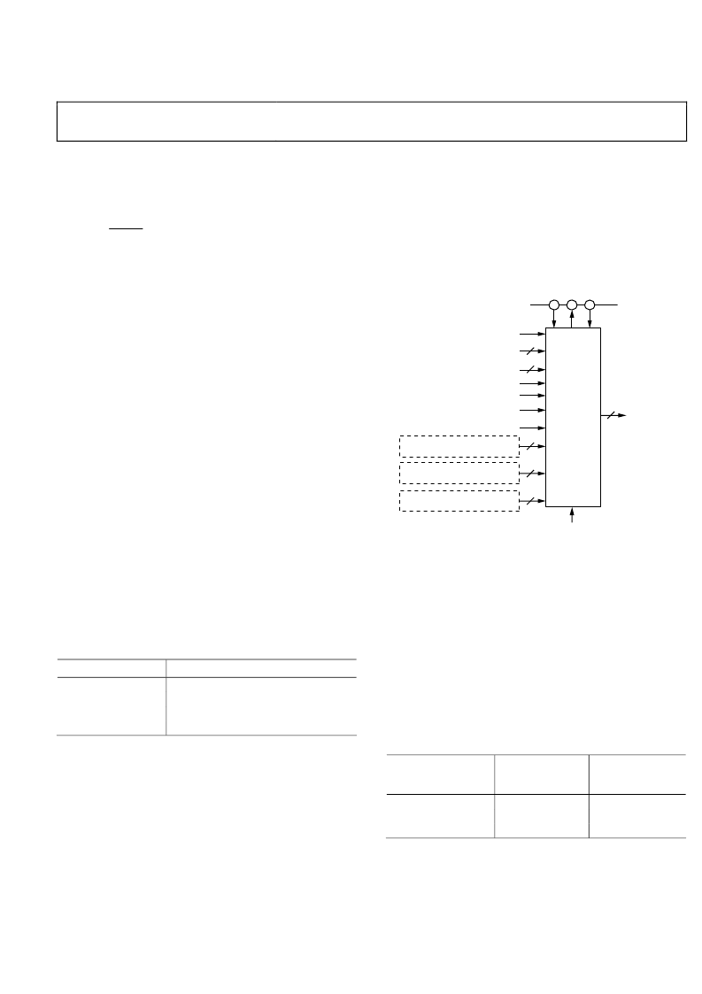
DIGITAL RAMP GENERATOR (DRG)
DRG Overview
To sweep phase, frequency, or amplitude from a defined start
point to a defined endpoint, a completely digital, digital ramp
generator is included in the AD9910. The DRG makes use of
nine control register bits, three external pins, two 64-bit
registers, and one 32-bit register (see Figure 37).
DIGITAL RAMP LIMIT REGISTER
D
DDS CLOCK
D
D
DIGITAL RAMP RATE REGISTER
DIGITAL RAMP STEP REGISTER
0
TO DDS
SIGNAL
CONTROL
PARAMETER
DIGITAL RAMP ENABLE
DROVER PIN ACTIVE
LOAD LRR AT I/O_UPDATE
CLEAR DIGITAL
RAMP ACCUMULATOR
AUTOCLEAR DIGITAL
RAMP ACCUMULATOR
64
64
DIGITAL RAMP DESTINATION
2
DIGITAL RAMP NO-DWELL
2
32
32
DIGITAL
RAMP
GENERATOR
62
61
63
Figure 37. Digital Ramp Block Diagram
The primary control for the DRG is the digital ramp enable bit.
When disabled, the other DRG input controls are ignored and the
internal clocks are shut down to conserve power.
The output of the DRG is a 32-bit unsigned data bus that can be
routed to any one of the three DDS signal control parameters, as
controlled by the two digital ramp destination bits in Control
Function Register 2 according to Table 11. The 32-bit output
bus is MSB-aligned with the 32-bit frequency parameter, the
16-bit phase parameter, or the 14-bit amplitude parameter, as
defined by the destination bits. When the destination is phase
or amplitude, the unused LSBs are ignored.
Table 11. Digital Ramp Destination
Digital Ramp
Destination Bits
CFR2<21:20>
00
01
1x
1
DDS signal
Control
Parameter
Frequency
Phase
Amplitude
Bits Assigned to
DDS Parameter
31:0
31:16
31:18
1
x = don’t care.
The ramp characteristics of the DRG are fully programmable. This
includes the upper and lower ramp limits, and independent control
of the step size and step rate for both the positive and negative slope
characteristics of the ramp. A detailed block diagram of the DRG
appears in Figure 38.
相關PDF資料 |
PDF描述 |
|---|---|
| AD9910_07 | 1 GSPS, 14-Bit, 3.3 V CMOS Direct Digital Synthesizer |
| AD9910BSVZ | 1 GSPS, 14-Bit, 3.3 V CMOS Direct Digital Synthesizer |
| AD9910BSVZ-REEL | 1 GSPS, 14-Bit, 3.3 V CMOS Direct Digital Synthesizer |
| AD9912 | 1 GSPS Direct Digital Synthesizer w/ 14-bit DAC |
| AD9913 | Low Power 250 MSPS 10-Bit DAC 1.8 V CMOS Direct Digital Synthesizer |
相關代理商/技術參數 |
參數描述 |
|---|---|
| AD9910/PCBZ | 功能描述:數據轉換 IC 開發工具 1GSPS 14 bit DDS w/ parallel input port RoHS:否 制造商:Texas Instruments 產品:Demonstration Kits 類型:ADC 工具用于評估:ADS130E08 接口類型:SPI 工作電源電壓:- 6 V to + 6 V |
| AD9910_07 | 制造商:AD 制造商全稱:Analog Devices 功能描述:1 GSPS, 14-Bit, 3.3 V CMOS Direct Digital Synthesizer |
| AD9910BSVZ | 功能描述:IC DDS 1GSPS 14BIT PAR 100TQFP RoHS:是 類別:集成電路 (IC) >> 接口 - 直接數字合成 (DDS) 系列:- 產品變化通告:Product Discontinuance 27/Oct/2011 標準包裝:2,500 系列:- 分辨率(位):10 b 主 fclk:25MHz 調節字寬(位):32 b 電源電壓:2.97 V ~ 5.5 V 工作溫度:-40°C ~ 85°C 安裝類型:表面貼裝 封裝/外殼:16-TSSOP(0.173",4.40mm 寬) 供應商設備封裝:16-TSSOP 包裝:帶卷 (TR) |
| AD9910BSVZ | 制造商:Analog Devices 功能描述:IC DDS 1GHZ TQFP-100 制造商:Analog Devices 功能描述:IC, DDS, 1GHZ, TQFP-100 |
| AD9910BSVZ-REEL | 功能描述:IC DDS 1GSPS 14BIT PAR 100TQFP RoHS:是 類別:集成電路 (IC) >> 接口 - 直接數字合成 (DDS) 系列:- 產品變化通告:Product Discontinuance 27/Oct/2011 標準包裝:2,500 系列:- 分辨率(位):10 b 主 fclk:25MHz 調節字寬(位):32 b 電源電壓:2.97 V ~ 5.5 V 工作溫度:-40°C ~ 85°C 安裝類型:表面貼裝 封裝/外殼:16-TSSOP(0.173",4.40mm 寬) 供應商設備封裝:16-TSSOP 包裝:帶卷 (TR) |
發布緊急采購,3分鐘左右您將得到回復。