- 您現在的位置:買賣IC網 > PDF目錄373970 > AD9910 (Analog Devices, Inc.) 1 GSPS, 14-Bit, 3.3 V CMOS Direct Digital Synthesizer PDF資料下載
參數資料
| 型號: | AD9910 |
| 廠商: | Analog Devices, Inc. |
| 元件分類: | XO, clock |
| 英文描述: | 1 GSPS, 14-Bit, 3.3 V CMOS Direct Digital Synthesizer |
| 中文描述: | 1 GSPS的,14位,3.3伏的CMOS直接數字頻率合成 |
| 文件頁數: | 25/60頁 |
| 文件大小: | 764K |
| 代理商: | AD9910 |
第1頁第2頁第3頁第4頁第5頁第6頁第7頁第8頁第9頁第10頁第11頁第12頁第13頁第14頁第15頁第16頁第17頁第18頁第19頁第20頁第21頁第22頁第23頁第24頁當前第25頁第26頁第27頁第28頁第29頁第30頁第31頁第32頁第33頁第34頁第35頁第36頁第37頁第38頁第39頁第40頁第41頁第42頁第43頁第44頁第45頁第46頁第47頁第48頁第49頁第50頁第51頁第52頁第53頁第54頁第55頁第56頁第57頁第58頁第59頁第60頁
AD9910
ranges such that f
SYSCLK
falls within the specified range. Figure 33
and Figure 34 summarize these VCO ranges.
Rev. 0 | Page 25 of 60
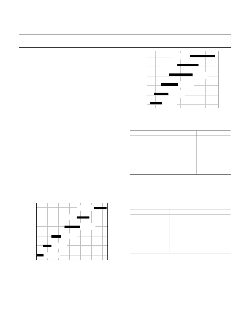
Figure 33 shows the boundaries of the VCO frequency ranges
over the full range of temperature and supply voltage variation
for all devices from the available population. The implication is
that multiple devices chosen at random from the population and
operated under widely varying conditions may require different
values to be programmed into CFR3<26:24> to operate at the
same frequency. For example, Part A chosen randomly from the
population, operating in an ambient temperature of 10°C with
a system clock frequency of 900 MHz may require CFR3<26:24>
to be set to 100b. Whereas Part B chosen randomly from the
population, operating in an ambient temperature of 90°C with a
system clock frequency of 900 MHz may require CFR3<26:24>
to be set to 101b. If a frequency plan is chosen such that the
system clock frequency operates within one set of boundaries
(as shown in Figure 33), the required value in CFR3<26:24> is
consistent from part to part.
Figure 34 shows the boundaries of the VCO frequency ranges
over the full range of temperature and supply voltage variation
for an individual device selected from the population. Figure 34
shows that the VCO frequency ranges for a single device always
overlap when operated over the full range of conditions.
In conclusion, if a user wants to retain a single default value for
CFR3<26:24>, a frequency that falls into one of the ranges
found in Figure 33 should be selected. Additionally, for any
given individual device the VCO frequency ranges overlap,
meaning that any given device exhibits no gaps in its frequency
coverage across VCO ranges over the full range of conditions.
0
VCO0
VCO1
VCO2
VCO3
VCO4
VCO5
395
495
595
695
(MHz)
795
895
995
FLOW = 400
FHIGH = 460
FLOW = 455
FHIGH = 530
FLOW = 530
FHIGH = 615
FLOW = 760
FHIGH = 875
FLOW = 920
FHIGH = 1030
FLOW = 650
FHIGH = 790
Figure 33. VCO Ranges Including Atypical Wafer Process Skew
335
435
535
635
735
(MHz)
835
935
1035
1135
VCO0
VCO1
VCO2
VCO3
VCO4
VCO5
0
FLOW = 370
FHIGH = 510
FLOW = 420
FHIGH = 590
FLOW = 500
FHIGH = 700
FLOW = 700
FHIGH = 950
FLOW = 820
FHIGH = 1150
FLOW = 600
FHIGH = 880
Figure 34. Typical VCO Ranges
Table 8. VCO Range Bit Settings
VCO SEL BITS (CFR3<26:24>)
000
001
010
011
100
101
110
111
PLL Charge Pump
The charge pump current (I
CP
) is programmable to provide the
user with additional flexibility to optimize the PLL performance.
Table 9 lists the bit settings vs. the nominal charge pump
current.
VCO Range
VCO0
VCO1
VCO2
VCO3
VCO4
VCO5
PLL Bypassed
PLL Bypassed
Table 9. PLL Charge Pump Current
I
CP
(CFR3<21:19>)
000
001
010
011
100
101
110
111
Charge Pump Current
(I
CP
in μA)
212
237
262
287
312
337
363
387
External PLL Loop Filter Components
The PLL_LOOP_FILTER pin provides a connection interface to
attach the external loop filter components. The ability to use
custom loop filter components gives the user more flexibility to
optimize the PLL performance. The PLL and external loop filter
components are shown in Figure 35.
相關PDF資料 |
PDF描述 |
|---|---|
| AD9910_07 | 1 GSPS, 14-Bit, 3.3 V CMOS Direct Digital Synthesizer |
| AD9910BSVZ | 1 GSPS, 14-Bit, 3.3 V CMOS Direct Digital Synthesizer |
| AD9910BSVZ-REEL | 1 GSPS, 14-Bit, 3.3 V CMOS Direct Digital Synthesizer |
| AD9912 | 1 GSPS Direct Digital Synthesizer w/ 14-bit DAC |
| AD9913 | Low Power 250 MSPS 10-Bit DAC 1.8 V CMOS Direct Digital Synthesizer |
相關代理商/技術參數 |
參數描述 |
|---|---|
| AD9910/PCBZ | 功能描述:數據轉換 IC 開發工具 1GSPS 14 bit DDS w/ parallel input port RoHS:否 制造商:Texas Instruments 產品:Demonstration Kits 類型:ADC 工具用于評估:ADS130E08 接口類型:SPI 工作電源電壓:- 6 V to + 6 V |
| AD9910_07 | 制造商:AD 制造商全稱:Analog Devices 功能描述:1 GSPS, 14-Bit, 3.3 V CMOS Direct Digital Synthesizer |
| AD9910BSVZ | 功能描述:IC DDS 1GSPS 14BIT PAR 100TQFP RoHS:是 類別:集成電路 (IC) >> 接口 - 直接數字合成 (DDS) 系列:- 產品變化通告:Product Discontinuance 27/Oct/2011 標準包裝:2,500 系列:- 分辨率(位):10 b 主 fclk:25MHz 調節字寬(位):32 b 電源電壓:2.97 V ~ 5.5 V 工作溫度:-40°C ~ 85°C 安裝類型:表面貼裝 封裝/外殼:16-TSSOP(0.173",4.40mm 寬) 供應商設備封裝:16-TSSOP 包裝:帶卷 (TR) |
| AD9910BSVZ | 制造商:Analog Devices 功能描述:IC DDS 1GHZ TQFP-100 制造商:Analog Devices 功能描述:IC, DDS, 1GHZ, TQFP-100 |
| AD9910BSVZ-REEL | 功能描述:IC DDS 1GSPS 14BIT PAR 100TQFP RoHS:是 類別:集成電路 (IC) >> 接口 - 直接數字合成 (DDS) 系列:- 產品變化通告:Product Discontinuance 27/Oct/2011 標準包裝:2,500 系列:- 分辨率(位):10 b 主 fclk:25MHz 調節字寬(位):32 b 電源電壓:2.97 V ~ 5.5 V 工作溫度:-40°C ~ 85°C 安裝類型:表面貼裝 封裝/外殼:16-TSSOP(0.173",4.40mm 寬) 供應商設備封裝:16-TSSOP 包裝:帶卷 (TR) |
發布緊急采購,3分鐘左右您將得到回復。