- 您現在的位置:買賣IC網 > PDF目錄373970 > AD9910 (Analog Devices, Inc.) 1 GSPS, 14-Bit, 3.3 V CMOS Direct Digital Synthesizer PDF資料下載
參數資料
| 型號: | AD9910 |
| 廠商: | Analog Devices, Inc. |
| 元件分類: | XO, clock |
| 英文描述: | 1 GSPS, 14-Bit, 3.3 V CMOS Direct Digital Synthesizer |
| 中文描述: | 1 GSPS的,14位,3.3伏的CMOS直接數字頻率合成 |
| 文件頁數: | 19/60頁 |
| 文件大小: | 764K |
| 代理商: | AD9910 |
第1頁第2頁第3頁第4頁第5頁第6頁第7頁第8頁第9頁第10頁第11頁第12頁第13頁第14頁第15頁第16頁第17頁第18頁當前第19頁第20頁第21頁第22頁第23頁第24頁第25頁第26頁第27頁第28頁第29頁第30頁第31頁第32頁第33頁第34頁第35頁第36頁第37頁第38頁第39頁第40頁第41頁第42頁第43頁第44頁第45頁第46頁第47頁第48頁第49頁第50頁第51頁第52頁第53頁第54頁第55頁第56頁第57頁第58頁第59頁第60頁
AD9910
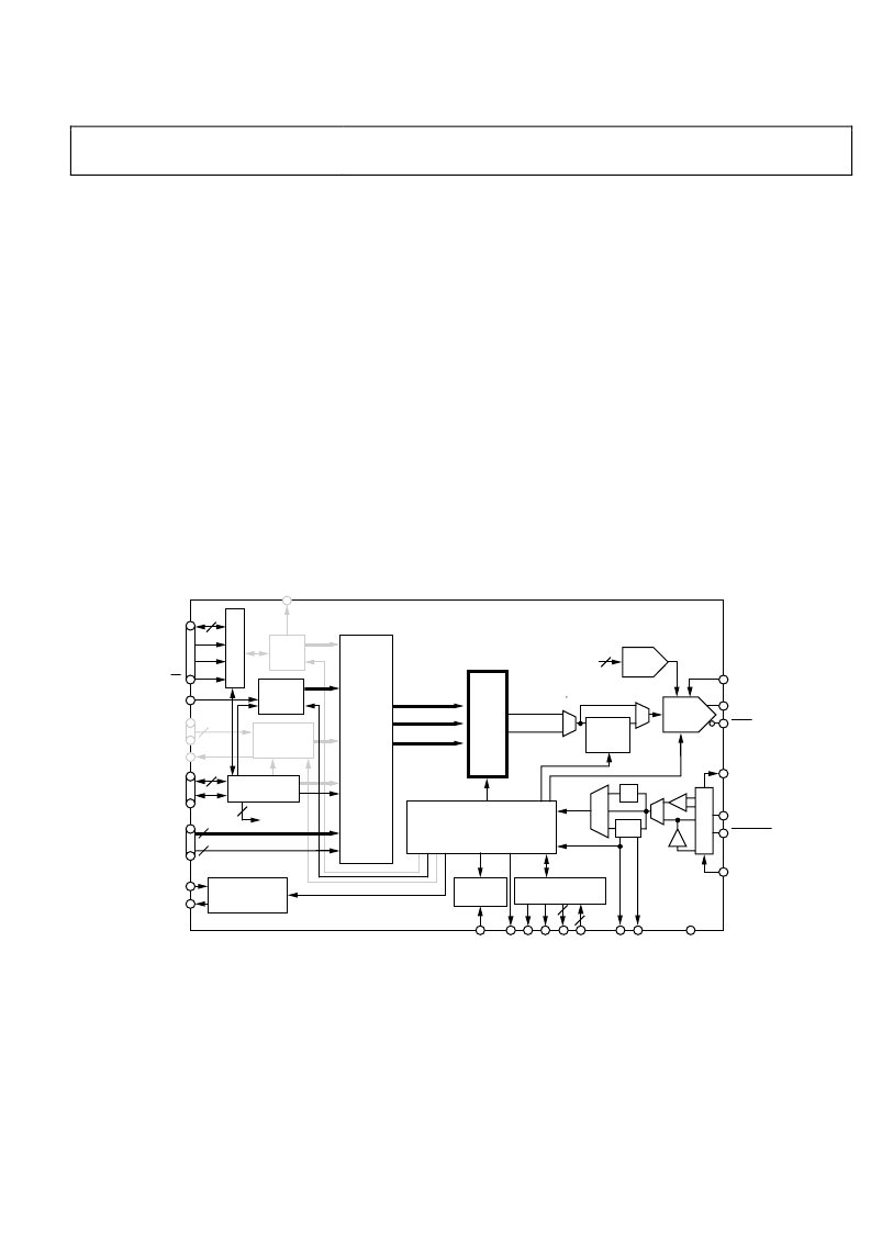
PARALLEL DATA PORT MODULATION MODE
In parallel data port modulation mode (Figure 25), the
modulated DDS signal control parameter(s) are supplied
directly from the 18-bit parallel data port.
Rev. 0 | Page 19 of 60
The data port is partitioned into two sections. The 16 MSBs
make up a 16-bit data-word (D<15:0> pins) and the 2 LSBs
make up a 2-bit destination word (F<1:0> pins). The destination
word defines how the 16-bit data-word is applied to the DDS
signal control parameters. Table 4 defines the relationship
between the destination bits, the partitioning of the 16-bit
data-word, and the destination of the data (in terms of the
DDS signal control parameters). Formatting of the 16-bit
data-word is unsigned binary, regardless of the destination.
When the destination bits indicate that the data-word is
destined as a DDS frequency parameter, the 16-bit data-word
serves as an offset to the 32-bit frequency tuning word in the
FTW register. This means that the 16-bit data-word must
somehow be properly aligned with the 32-bit frequency
parameter. This is accomplished by means of the 4-bit FM gain
word in the programming registers. The FM gain word allows
RAM_SWP_OVR
the user to apply a weighting factor to the 16-bit data-word. In
the default state (0), the 16-bit data-word and the 32-bit word in
the FTW register are LSB aligned. Each increment in the value
of the FM gain word shifts the 16-bit data-word to the left
relative to the 32-bit word in the FTW register, increasing the
influence of the 16-bit data-word on the frequency defined by
the FTW register by a factor of two. The FM gain word effectively
controls the frequency range spanned by the data-word.
Parallel Data Clock (PDCLK)
The AD9910 generates a clock signal on the PDCLK pin that
runs at of the DAC sample rate (the sample rate of the par-
allel data port). PDCLK serves as a data clock for the parallel
port. By default, each rising edge of PDCLK is used to latch the
18 bits of user-supplied data into the data port. The edge polarity
can be changed through the PDCLK invert bit. Furthermore,
the PDCLK output signal can be switched off using the PDCLK
enable bit. However, even though the output signal is switched
off, it continues to operate internally using the internal PDCLK
timing to capture the data at the parallel port. Note that PDCLK
is Logic 0 when disabled.
0
16
PARALLEL
INPUT
PDCLK
SCLK
SDIO
I/O_RESET
PROFILE
I/O_UPDATE
RAM
POWER
DOWN
CONTROL
E
DAC_RSET
IOUT
IOUT
CS
TxENABLE
DAC FSC
OSK
A
θ
INVERSE
SINC
FILTER
CLOCK
AMPLITUDE (A)
FREQUENCY (
ω
)
PHASE (
θ
)
DIGITAL
RAMP
GENERATOR
8
DAC FSC
8
2
2
MULTICHIP
SYNCHRONIZATION
SYSCLK
PLL
÷2
C
REF_CLK
REF_CLK
REFCLK_OUT
XTAL_SEL
PARALLEL DATA
TIMING AND
CONTROL
S
2
AD9910
PROGRAMMING
REGISTERS
OUTPUT
SHIFT
KEYING
DATA
ROUTE
AND
PARTITION
CONTROL
3
INTERNAL CLOCK TIMING
AND CONTROL
ω
Acos (
ω
t+
θ
)
Asin (
ω
t+
θ
)
S
S
S
S
P
P
M
2
2
DDS
AUX
DAC
8-BIT
DAC
14-BIT
DRCTL
DRHOLD
DROVER
S
Figure 25. Parallel Data Port Modulation Mode
相關PDF資料 |
PDF描述 |
|---|---|
| AD9910_07 | 1 GSPS, 14-Bit, 3.3 V CMOS Direct Digital Synthesizer |
| AD9910BSVZ | 1 GSPS, 14-Bit, 3.3 V CMOS Direct Digital Synthesizer |
| AD9910BSVZ-REEL | 1 GSPS, 14-Bit, 3.3 V CMOS Direct Digital Synthesizer |
| AD9912 | 1 GSPS Direct Digital Synthesizer w/ 14-bit DAC |
| AD9913 | Low Power 250 MSPS 10-Bit DAC 1.8 V CMOS Direct Digital Synthesizer |
相關代理商/技術參數 |
參數描述 |
|---|---|
| AD9910/PCBZ | 功能描述:數據轉換 IC 開發工具 1GSPS 14 bit DDS w/ parallel input port RoHS:否 制造商:Texas Instruments 產品:Demonstration Kits 類型:ADC 工具用于評估:ADS130E08 接口類型:SPI 工作電源電壓:- 6 V to + 6 V |
| AD9910_07 | 制造商:AD 制造商全稱:Analog Devices 功能描述:1 GSPS, 14-Bit, 3.3 V CMOS Direct Digital Synthesizer |
| AD9910BSVZ | 功能描述:IC DDS 1GSPS 14BIT PAR 100TQFP RoHS:是 類別:集成電路 (IC) >> 接口 - 直接數字合成 (DDS) 系列:- 產品變化通告:Product Discontinuance 27/Oct/2011 標準包裝:2,500 系列:- 分辨率(位):10 b 主 fclk:25MHz 調節字寬(位):32 b 電源電壓:2.97 V ~ 5.5 V 工作溫度:-40°C ~ 85°C 安裝類型:表面貼裝 封裝/外殼:16-TSSOP(0.173",4.40mm 寬) 供應商設備封裝:16-TSSOP 包裝:帶卷 (TR) |
| AD9910BSVZ | 制造商:Analog Devices 功能描述:IC DDS 1GHZ TQFP-100 制造商:Analog Devices 功能描述:IC, DDS, 1GHZ, TQFP-100 |
| AD9910BSVZ-REEL | 功能描述:IC DDS 1GSPS 14BIT PAR 100TQFP RoHS:是 類別:集成電路 (IC) >> 接口 - 直接數字合成 (DDS) 系列:- 產品變化通告:Product Discontinuance 27/Oct/2011 標準包裝:2,500 系列:- 分辨率(位):10 b 主 fclk:25MHz 調節字寬(位):32 b 電源電壓:2.97 V ~ 5.5 V 工作溫度:-40°C ~ 85°C 安裝類型:表面貼裝 封裝/外殼:16-TSSOP(0.173",4.40mm 寬) 供應商設備封裝:16-TSSOP 包裝:帶卷 (TR) |
發布緊急采購,3分鐘左右您將得到回復。