- 您現在的位置:買賣IC網 > PDF目錄373970 > AD9910 (Analog Devices, Inc.) 1 GSPS, 14-Bit, 3.3 V CMOS Direct Digital Synthesizer PDF資料下載
參數資料
| 型號: | AD9910 |
| 廠商: | Analog Devices, Inc. |
| 元件分類: | XO, clock |
| 英文描述: | 1 GSPS, 14-Bit, 3.3 V CMOS Direct Digital Synthesizer |
| 中文描述: | 1 GSPS的,14位,3.3伏的CMOS直接數字頻率合成 |
| 文件頁數: | 36/60頁 |
| 文件大小: | 764K |
| 代理商: | AD9910 |
第1頁第2頁第3頁第4頁第5頁第6頁第7頁第8頁第9頁第10頁第11頁第12頁第13頁第14頁第15頁第16頁第17頁第18頁第19頁第20頁第21頁第22頁第23頁第24頁第25頁第26頁第27頁第28頁第29頁第30頁第31頁第32頁第33頁第34頁第35頁當前第36頁第37頁第38頁第39頁第40頁第41頁第42頁第43頁第44頁第45頁第46頁第47頁第48頁第49頁第50頁第51頁第52頁第53頁第54頁第55頁第56頁第57頁第58頁第59頁第60頁
AD9910
Rev. 0 | Page 36 of 60
RAM_SWP_OVER
WAVEFORM START ADDRESS 0
WAVEFORM END ADDRESS 0
1
WAVEFORM START ADDRESS 1
WAVEFORM END ADDRESS 1
1
WAVEFORM END ADDRESS 2
1
RAM PROFILE
0
1
2
WAVEFORM START ADDRESS 2
RAM
ADDRESS
I/O_UPDATE
Δ
t
0
Δ
t
1
Δ
t
2
1
2
3
4
5
6
7
0
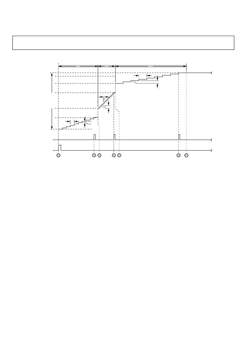
Figure 44. Internal Profile Control Timing Diagram (Burst)
The gray bar across the top indicates the time interval over
which the designated profile is in effect. The circled numbers
indicate specific events as follows:
Event 1—An I/O update registers the Internal Profile Control
bits (in Control Function Register 1) are as 0010. The
RAM_SWP_OVR pin is set to Logic 0. The state machine is
initialized to the waveform start address of RAM Profile 0 and
begins incrementing through the address range for RAM
Profile 0 at intervals of Δt
0
(as specified by the address step rate
for RAM Profile 0).
Event 2—The state machine reaches the waveform end address
of RAM Profile 0 and the RAM_SWP_OVR pin generates a
positive pulse spanning two DDS clock cycles.
Event 3—Having reached the waveform end address of RAM
Profile 0, the next expiration of the internal timer causes the
state machine to advance to RAM Profile 1. The state machine
is initialized to the waveform start address of RAM Profile 1
and begins incrementing through the address range for RAM
Profile 1 at intervals of Δt
1
.
Event 4—The state machine reaches the waveform end address
of RAM Profile 1 and the RAM_SWP_OVR pin generates a
positive pulse spanning two DDS clock cycles.
Event 5—Having reached the waveform end address of RAM
Profile 1, the next expiration of the internal timer causes the
state machine to advance to RAM Profile 2. The state machine
initializes to the waveform start address of RAM Profile 2 and
begins incrementing through the address range for RAM
Profile 2 at intervals of Δt
2
.
Event 6—The state machine reaches the waveform end address of
RAM Profile 2 and the RAM_SWP_OVR pin generates a positive
pulse spanning two DDS clock cycles.
Event 7—Having reached the waveform end address of RAM
Profile 2, the next expiration of the internal timer causes the
state machine to halt and marks completion of the burst
waveform generation process.
相關PDF資料 |
PDF描述 |
|---|---|
| AD9910_07 | 1 GSPS, 14-Bit, 3.3 V CMOS Direct Digital Synthesizer |
| AD9910BSVZ | 1 GSPS, 14-Bit, 3.3 V CMOS Direct Digital Synthesizer |
| AD9910BSVZ-REEL | 1 GSPS, 14-Bit, 3.3 V CMOS Direct Digital Synthesizer |
| AD9912 | 1 GSPS Direct Digital Synthesizer w/ 14-bit DAC |
| AD9913 | Low Power 250 MSPS 10-Bit DAC 1.8 V CMOS Direct Digital Synthesizer |
相關代理商/技術參數 |
參數描述 |
|---|---|
| AD9910/PCBZ | 功能描述:數據轉換 IC 開發工具 1GSPS 14 bit DDS w/ parallel input port RoHS:否 制造商:Texas Instruments 產品:Demonstration Kits 類型:ADC 工具用于評估:ADS130E08 接口類型:SPI 工作電源電壓:- 6 V to + 6 V |
| AD9910_07 | 制造商:AD 制造商全稱:Analog Devices 功能描述:1 GSPS, 14-Bit, 3.3 V CMOS Direct Digital Synthesizer |
| AD9910BSVZ | 功能描述:IC DDS 1GSPS 14BIT PAR 100TQFP RoHS:是 類別:集成電路 (IC) >> 接口 - 直接數字合成 (DDS) 系列:- 產品變化通告:Product Discontinuance 27/Oct/2011 標準包裝:2,500 系列:- 分辨率(位):10 b 主 fclk:25MHz 調節字寬(位):32 b 電源電壓:2.97 V ~ 5.5 V 工作溫度:-40°C ~ 85°C 安裝類型:表面貼裝 封裝/外殼:16-TSSOP(0.173",4.40mm 寬) 供應商設備封裝:16-TSSOP 包裝:帶卷 (TR) |
| AD9910BSVZ | 制造商:Analog Devices 功能描述:IC DDS 1GHZ TQFP-100 制造商:Analog Devices 功能描述:IC, DDS, 1GHZ, TQFP-100 |
| AD9910BSVZ-REEL | 功能描述:IC DDS 1GSPS 14BIT PAR 100TQFP RoHS:是 類別:集成電路 (IC) >> 接口 - 直接數字合成 (DDS) 系列:- 產品變化通告:Product Discontinuance 27/Oct/2011 標準包裝:2,500 系列:- 分辨率(位):10 b 主 fclk:25MHz 調節字寬(位):32 b 電源電壓:2.97 V ~ 5.5 V 工作溫度:-40°C ~ 85°C 安裝類型:表面貼裝 封裝/外殼:16-TSSOP(0.173",4.40mm 寬) 供應商設備封裝:16-TSSOP 包裝:帶卷 (TR) |
發布緊急采購,3分鐘左右您將得到回復。