- 您現(xiàn)在的位置:買賣IC網(wǎng) > PDF目錄373969 > AD9874 (ANALOG DEVICES INC) IF Digitizing Subsystem PDF資料下載
參數(shù)資料
| 型號: | AD9874 |
| 廠商: | ANALOG DEVICES INC |
| 元件分類: | 通信及網(wǎng)絡(luò) |
| 英文描述: | IF Digitizing Subsystem |
| 中文描述: | SPECIALTY TELECOM CIRCUIT, PQFP48 |
| 封裝: | 1.40 MM HEIGHT, PLASTIC, TQFP-48 |
| 文件頁數(shù): | 15/40頁 |
| 文件大小: | 744K |
| 代理商: | AD9874 |
第1頁第2頁第3頁第4頁第5頁第6頁第7頁第8頁第9頁第10頁第11頁第12頁第13頁第14頁當前第15頁第16頁第17頁第18頁第19頁第20頁第21頁第22頁第23頁第24頁第25頁第26頁第27頁第28頁第29頁第30頁第31頁第32頁第33頁第34頁第35頁第36頁第37頁第38頁第39頁第40頁
REV. 0
AD9874
–15–
SYNCHRONOUS SERIAL INTERFACE (SSI)
The AD9874 provides a high degree of programmability of its
SSI output data format, control signals, and timing parameters
to accommodate various digital interfaces. In a 3-wire digital
interface, the AD9874 provides a frame sync signal (FS), a
clock output (CLKOUT), and a serial data stream (DOUTA)
signal to the host device. In a 2-wire interface, the frame sync
information is embedded into the data stream, thus only a
CLKOUT and DOUTA output signal are provided to the host
device. The SSI control registers are SSICRA, SSICRB, and
SSIORD. Table III shows the different bit fields associated with
these registers.
The primary output of the AD9874 is the converted I and Q
demodulated signal available from the SSI port as a serial bit
stream contained within a frame. The output frame rate is equal
to the modulator clock frequency (f
CLK
) divided by the digital
filter’s decimation factor that is programmed in the Decimator
Register (0x07). The bit stream consists of an I word followed
by a Q word, where each word is either 24 bits or 16 bits long
and is given MSB first in two’s complement form. Two optional
bytes may also be included within the SSI frame following the
Q word. One byte contains the AGC attenuation and the other
byte contains both a count of modulator reset events and an
estimate of the received signal amplitude (relative to full scale
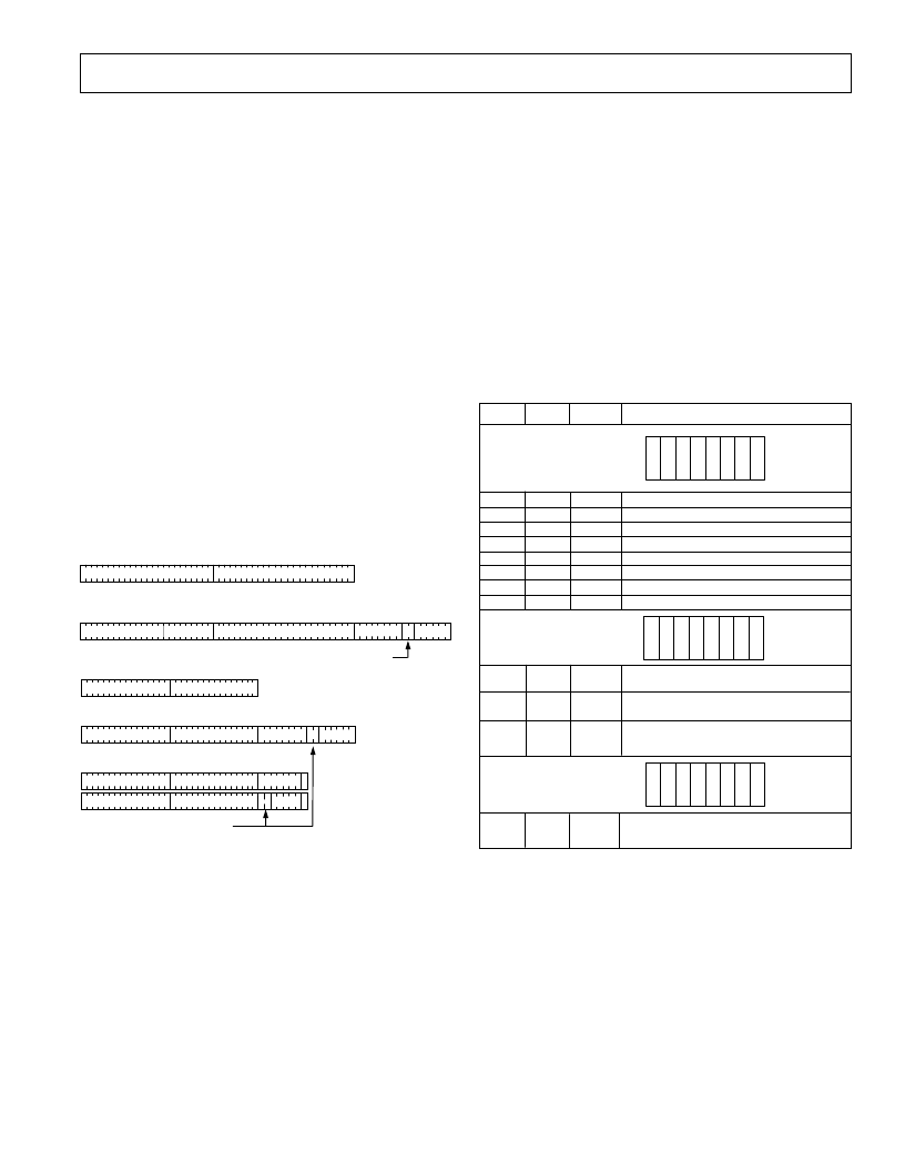
of the AD9874’s ADC). Figure 2 illustrates the structure of the
SSI data frames in a number of SSI modes.
16-Bit I AND Q, EAGC = 0, AAGC = X:32 DATA BITS
16-Bit I AND Q, EAGC = 1, AAGC = 0:48 DATA BITS
16-Bit I AND Q, EAGC = 1, AAGC = 1:40 DATA BITS
I (15:0)
Q (15:0)
I (15:0)
Q (15:0)
ATTN (7:0)
I (15:0)
Q (15:0)
0
I (15:0)
Q (15:0)
1
RESET COUNT
I (24:0)
Q (24:0)
24-Bit I AND Q, EAGC = 0, AAGC = X: 48 DATA BITS
ATTN (7:1)
SSI(5:1)
SSI(5:0)
I (24:0)
Q (24:0)
SSI(5:0)
RESET COUNT
ATTN (7:0)
24-Bit I AND Q, EAGC = 1, AAGC = 0:64 DATA BITS
Figure 2. SSI Frame Structure
The two optional bytes are output if the EAGC bit of SSICRA
is set. The first byte contains the 8-bit attenuation setting (0 = no
attenuation, 255 = 24 dB of attenuation), while the second
byte
contains a 2-bit reset field and 6-bit received signal
strength
signal field. The reset field contains the number of
modulator
reset events since the last report, saturating at 3. The
received
signal strength (RSSI) field is a linear estimate of the signal
strength at the output of the first decimation stage; 60 corresponds
to a full-scale signal.
The two optional bytes follow the I and Q data as a 16-bit word
providing that the AAGC bit of SSICRA is not set. If the
AAGC bit is set, the two bytes follow the I and Q data in an
alternating fashion. In this alternate AGC data mode, the LSB
of the byte containing the AGC attenuation is a 0, while the LSB
of the byte containing reset and RSSI information is always a 1.
In a 2-wire interface, the embedded frame sync bit (EFS) within
the SSICRA Register is set to 1. In this mode, the framing infor-
mation is embedded in the data stream with each eight bits of
data surrounded by a start bit (low) and a stop bit (high), and
each frame ends with at least 10 high bits. FS remains either
low or three-stated (default) depending on the state of the
SFST bit. Other control bits can be used to invert the frame
sync (SFSI), to delay the frame sync pulse by one clock
period (SLFS), to invert the clock (SCKI), or to three-state the
clock (SCKT). Note that if EFS is set, SLFS is a don’t care.
Name Width Default
Description
SSICRA (ADDR = 0x18)
AAGC
EAGC
EFS
SFST
SFSI
SLFS
SCKT
SCKI
1
1
1
1
1
1
1
1
Alternate AGC Data Bytes
Embed AGC Data
Embed Frame Sync
Three-State Frame Sync
Invert Frame Sync
Late Frame Sync (1 = Late, 0 = Early)
Three-State CLKOUT
Invert CLKOUT
SSICRB (ADDR = 0x19)
DS
3
FS, CLKOUT, and DOUT Drive
Strength
7
DW
1
Output Bit Rate Divisor
fCLKOUT
=
fCLK
/SSIORD
0
1
0
1
0
0
0
0
0
A
E
E
S
S
S
S
S
D
D
D
D
D
SSIORD (ADDR = 0x1A)
I/Q data-word width (0 = 16 bit, 1 bit–24 bit)
Automatically 16-bit when the AGCV=1
4
1
D
D
D
DIV
4
4_SPI
0
Enable 4-Wire SPI Interface for SPI Read
operation via DOUTB
1
The SSIORD Register controls the output bit rate (f
CLKOUT
) of
the serial bit stream.
f
CLKOUT
can be set to equal the modulator
clock frequency (f
CLK
) or an integer fraction of it. It
is equal to
f
CLK
divided by the contents of the SSIORD Register. Note,
f
CLKOUT
should be chosen such that it does not introduce harmful
spurs within the pass band of the target signal. Users must verify
that the output bit rate is sufficient to accommodate the required
number of bits per frame for a selected word size and decimation
factor. Idle (high) bits are used to fill out each frame.
Table III. SSI Control Registers
相關(guān)PDF資料 |
PDF描述 |
|---|---|
| AD9874BST | IF Digitizing Subsystem |
| AD9874EB | IF Digitizing Subsystem |
| AD9875BSTRL | Broadband Modem Mixed-Signal Front End |
| AD9875 | Broadband Modem Mixed-Signal Front End |
| AD9875-EB | Broadband Modem Mixed-Signal Front End |
相關(guān)代理商/技術(shù)參數(shù) |
參數(shù)描述 |
|---|---|
| AD9874ABST | 功能描述:IC IF DIGIT SUBSYSTEM 48-LQFP RoHS:否 類別:RF/IF 和 RFID >> RF 其它 IC 和模塊 系列:- 標準包裝:100 系列:* |
| AD9874ABST | 制造商:Analog Devices 功能描述:IF DIGITIZING SYBSYSTEM ((NW)) 制造商:Analog Devices 功能描述:IC, IF DIGITIZING SUBSYSTEM, LQFP-48 |
| AD9874ABST | 制造商:Analog Devices 功能描述:IC IF DIG SUBSYSTEM |
| AD9874ABSTRL | 功能描述:IC IF DIGIT SUBSYSTEM 48-LQFP RoHS:否 類別:RF/IF 和 RFID >> RF 其它 IC 和模塊 系列:- 標準包裝:100 系列:* |
| AD9874ABSTZ | 制造商:AD 制造商全稱:Analog Devices 功能描述:IF Digitizing Subsystem |
發(fā)布緊急采購,3分鐘左右您將得到回復。