- 您現在的位置:買賣IC網 > PDF目錄373969 > AD9874 (ANALOG DEVICES INC) IF Digitizing Subsystem PDF資料下載
參數資料
| 型號: | AD9874 |
| 廠商: | ANALOG DEVICES INC |
| 元件分類: | 通信及網絡 |
| 英文描述: | IF Digitizing Subsystem |
| 中文描述: | SPECIALTY TELECOM CIRCUIT, PQFP48 |
| 封裝: | 1.40 MM HEIGHT, PLASTIC, TQFP-48 |
| 文件頁數: | 23/40頁 |
| 文件大小: | 744K |
| 代理商: | AD9874 |
第1頁第2頁第3頁第4頁第5頁第6頁第7頁第8頁第9頁第10頁第11頁第12頁第13頁第14頁第15頁第16頁第17頁第18頁第19頁第20頁第21頁第22頁當前第23頁第24頁第25頁第26頁第27頁第28頁第29頁第30頁第31頁第32頁第33頁第34頁第35頁第36頁第37頁第38頁第39頁第40頁
REV. 0
AD9874
–23–
Based on these characterization curves, a LNA/mixer bias setting
of 3_3 is suitable for most applications since it will provide the
greatest dynamic range in the presence of multiple unfiltered
interferers. However, portable radio applications demanding the
lowest possible power may benefit by changing the LNA/mixer
bias setting based on the received signal strength power (i.e., RSSI)
available from the SSI output data. For instance, selecting an
LNA_Mixer bias setting of 1_2 for nominal input strength condi-
tions (i.e., <–45 dBm) would result in a 4 mA current savings
(i.e., 18% reduction). If the signal exceeds this level, a bias setting
of 3_3 could be selected. Lastly, refer to the Typical Performance
Characteristics (TPCs) for more performance graphs character-
izing the LNA and mixer’s effect upon the AD9874’s noise and
linearity performance under different operating conditions.
0
0
–1
–2
–3
–5
d
100
200
FREQUENCY – MHz
300
400
500
–4
–6
–7
–8
LNA_MIXER
1_2 SETTING
LNA_MIXER
3_3 SETTING
Figure 11c. LNA/Mixer Frequency Response vs. Bias Setting
A 16 dB step attenuator is also included within the LNA/mixer
circuitry to prevent large signals (i.e., > –18 dBm) from overdriving
the - modulator. In such instances, the - modulator will
become unstable, thus severely desensitizing the receiver. The
16 dB step attenuator can be invoked by setting the ATTEN bit
(Register 0x03, Bit 7), causing the mixer gain to be reduced by
16 dB. The 16 dB step attenuator could be used in applications
in which a potential target or blocker signal could exceed the IF
input clip point. Although the LNA will be driven into compression,
it may still be possible to recover the desired signal if it is FM.
Refer to TPC 7c to see the gain compression characteristics of the
LNA and mixer with the 16 dB attenuator enabled.
Table IX. SPI Registers Associated with LNA/Mixer
Address
(Hex)
Bit
Breakdown
Default
Value
Width
Name
0x00
0x01
0x01
0x03
(7:0)
(7:6)
(5:4)
(7)
8
2
2
1
0xFF
0
0
0
STBY
LNAB
MIXB
ATTEN
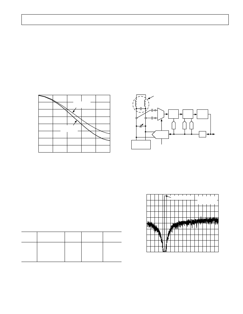
Band-Pass Sigma-Delta (
-
) ADC
The ADC of the AD9874 is shown in Figure 12. The ADC contains
a sixth order multibit band-pass - modulator that achieves very
high instantaneous dynamic range over a narrow frequency band.
The loop filter of the band-pass - modulator consists of two
continuous-time resonators followed by a discrete-time resonator,
with each resonator stage contributing a pair of complex poles.
The first resonator is an external LC tank, while the second is an
on-chip active RC filter. The output of the LC resonator is
ac-coupled to the second resonator input via 100 pF capacitors.
The center frequencies of these two continuous-time resonators
must be tuned to
f
CLK
/8 for the ADC to function properly. The
center frequency of the discrete-time resonator automatically scales
with
f
CLK
, thus no tuning is required.
TO DIGITAL
FILTER
SC
RESO-
NATOR
NINE-
LEVEL
FLASH
ESL
GAIN
CONTROL
MIXER
OUTPUT
EXTERNAL
LC
f
CLK
= 13 MSPS–26 MSPS
MXOP
MXON
IF2P
IF2N
RC
RESO-
NATOR
DAC1
Figure 12. Equivalent Circuit of Sixth Order
Band-Pass - Modulator
Figure 13a shows the measured power spectral density measured
at the output of the undecimated band-pass - modulator. Note,
the wide dynamic range achieved at the center frequency,
f
CLK
/8,
is achieved once the LC and RC resonators of the - modulator
have been successfully tuned. The out-of-band noise is removed
by the decimation filters following quadrature demodulation.
0
0
–10
–20
–30
–50
d
–40
FREQUENCY – MHz
–60
–70
–80
–90
–100
1
2
3
4
5
6
7
8
9
–2 dBFS OUTPUT
f
CLK
= 18MHz
NBW = 3.3kHz
Figure 13a. Measured Undecimated Spectral Output of
-
Modulator ADC with f
CLK
= 18 MSPS and Noise
Bandwidth of 3.3 kHz
相關PDF資料 |
PDF描述 |
|---|---|
| AD9874BST | IF Digitizing Subsystem |
| AD9874EB | IF Digitizing Subsystem |
| AD9875BSTRL | Broadband Modem Mixed-Signal Front End |
| AD9875 | Broadband Modem Mixed-Signal Front End |
| AD9875-EB | Broadband Modem Mixed-Signal Front End |
相關代理商/技術參數 |
參數描述 |
|---|---|
| AD9874ABST | 功能描述:IC IF DIGIT SUBSYSTEM 48-LQFP RoHS:否 類別:RF/IF 和 RFID >> RF 其它 IC 和模塊 系列:- 標準包裝:100 系列:* |
| AD9874ABST | 制造商:Analog Devices 功能描述:IF DIGITIZING SYBSYSTEM ((NW)) 制造商:Analog Devices 功能描述:IC, IF DIGITIZING SUBSYSTEM, LQFP-48 |
| AD9874ABST | 制造商:Analog Devices 功能描述:IC IF DIG SUBSYSTEM |
| AD9874ABSTRL | 功能描述:IC IF DIGIT SUBSYSTEM 48-LQFP RoHS:否 類別:RF/IF 和 RFID >> RF 其它 IC 和模塊 系列:- 標準包裝:100 系列:* |
| AD9874ABSTZ | 制造商:AD 制造商全稱:Analog Devices 功能描述:IF Digitizing Subsystem |
發布緊急采購,3分鐘左右您將得到回復。