- 您現在的位置:買賣IC網 > PDF目錄16699 > AFE7222EVM (Texas Instruments)EVAL MODULE FOR AFE7222 PDF資料下載
參數資料
| 型號: | AFE7222EVM |
| 廠商: | Texas Instruments |
| 文件頁數: | 102/106頁 |
| 文件大小: | 0K |
| 描述: | EVAL MODULE FOR AFE7222 |
| 標準包裝: | 1 |
| 主要目的: | 接口,模擬前端(AFE) |
| 嵌入式: | 否 |
| 已用 IC / 零件: | AFE7222 |
| 已供物品: | 板 |
| 其它名稱: | 296-30300 AFE7222EVM-ND |
第1頁第2頁第3頁第4頁第5頁第6頁第7頁第8頁第9頁第10頁第11頁第12頁第13頁第14頁第15頁第16頁第17頁第18頁第19頁第20頁第21頁第22頁第23頁第24頁第25頁第26頁第27頁第28頁第29頁第30頁第31頁第32頁第33頁第34頁第35頁第36頁第37頁第38頁第39頁第40頁第41頁第42頁第43頁第44頁第45頁第46頁第47頁第48頁第49頁第50頁第51頁第52頁第53頁第54頁第55頁第56頁第57頁第58頁第59頁第60頁第61頁第62頁第63頁第64頁第65頁第66頁第67頁第68頁第69頁第70頁第71頁第72頁第73頁第74頁第75頁第76頁第77頁第78頁第79頁第80頁第81頁第82頁第83頁第84頁第85頁第86頁第87頁第88頁第89頁第90頁第91頁第92頁第93頁第94頁第95頁第96頁第97頁第98頁第99頁第100頁第101頁當前第102頁第103頁第104頁第105頁第106頁
ADC_DCLKOUT
ADCDATA <11:0>
A
B
A
B
A
B
SLOS711B – NOVEMBER 2011 – REVISED MARCH 2012
Clocking:
By default, the device expects a differential clock on CLKINP and CLKINN. This differential clock is used
to drive both the ADC and DAC.
In case the clock source is single ended, then short CLKINN to a voltage of 0.95V and apply the single
ended clock source on CLKINP – alternatively, CLKINP can be driven with a voltage of 0.95V and the
single ended clock source can be applied on CLKINN.
A third alternative is to use the single ended clock buffer inside the device. This mode saves about 9 mW
of power since the differential clock buffer is shut down. By setting register (address 20A, Data 20), the
single ended clock buffer can be enabled. In that case, Pin 8 provides the single ended clock for the DAC
whereas Pin 9 provides the single ended clock for the ADC – if a single clock source is to be used for
both, then tie pins 8 and 9 to this clock source.
Biasing the ADC inputs:
The common mode of the ADC input pins should set to VCM, which is nominally 0.95V (measured after
programming the initialization registers). Deviating from this input common mode can cause degraded
performance. The full scale input swing on the inputs is 2 Volt differential peak-to-peak. When biased
optimally at 0.95V, the device gives a full scale output code when the positive input swings between
roughly 0.45V and 1.45V (and correspondingly the negative input swings between 1.45V and 0.45V). It is
recommended to operate the ADC at an input that is at least 1 dB below full scale.
ADC output format:
The ADC gives out a 12-bit output in 2s complement format. For the most negative input, the ADC gives
out a code of 100000000000. For the most positive input, the output code is 011111111111.
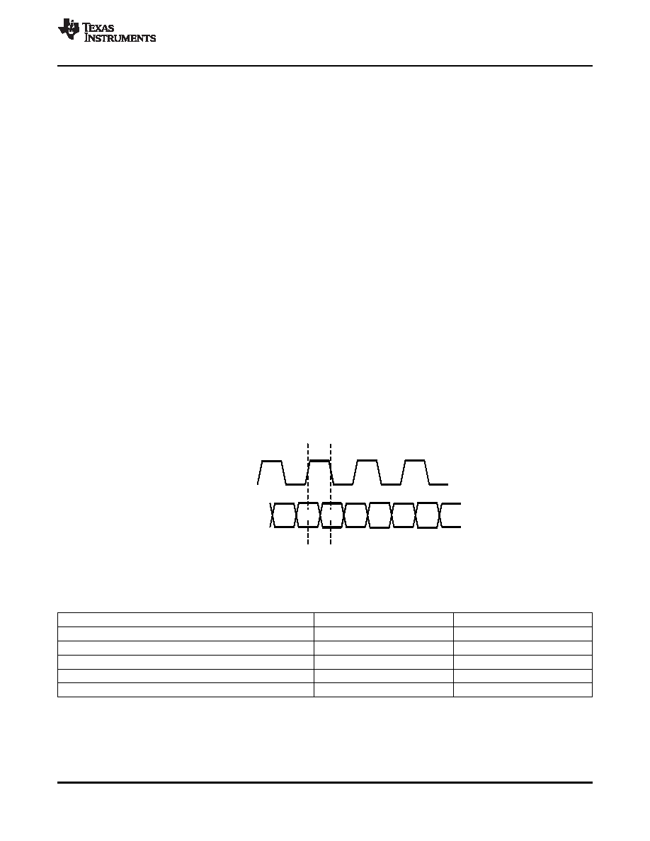
RX data output capture (CMOS mode) :
The RX output data format is DDR (Dual data rate) CMOS. The output of the ADC channel A can be
captured using the rising edge of ADC_DCLKOUT. The output of ADC channel B can be captured using
the falling edge of ADC_DCLKOUT. The clock rate of ADC_DCLKOUT matches with the input clock rate
(on CLKINP, CLKINN).
Figure 11-1. RX CMOS Output Interface
A variety of test patterns can be output by the device in order to debug issues with the capture. To enable
the test patterns, program register address 042, Data 08. Once this register is programmed, we can
change the output pattern as follows :
TO REPLACE NORMAL DATA WITH THE FOLLOWING
.. ON CHANNEL A WRITE
.. ON CHANNEL B WRITE
All bits 0
Address 031, Data 01
Address 037, Data 01
All bits 1
Address 031, Data 02
Address 037, Data 02
All bits toggle between 0 and 1
Address 031, Data 03
Address 037, Data 03
Linearly ramping code that ramps through min to max code
Address 031, Data 04
Address 037, Data 04
12-bit Custom code
Address 031, Data 05
Address 037, Data 05
The 12 bits for the custom code (C<11 :0>) can be set (common for Channel A and B) using the following
bits:
C<11> = Bit D5 of regster address 03F
C<10> = Bit D4 of regster address 03F
C<9> = Bit D3 of regster address 03F
Copyright 2011–2012, Texas Instruments Incorporated
QUICK GUIDE
95
相關PDF資料 |
PDF描述 |
|---|---|
| ECE-V1EA100NP | CAP ALUM 10UF 25V 20% SMD |
| 0210491116 | CABLE JUMPER 1.25MM .305M 39POS |
| UPM1J270MED1TD | CAP ALUM 27UF 63V 20% RADIAL |
| RNF-100-1-1/4-RD-SP | HEAT SHRINK TUBING |
| RNF-100-1-1/4-BU-SP | HEAT SHRINK TUBING |
相關代理商/技術參數 |
參數描述 |
|---|---|
| AFE7222IRGC25 | 功能描述:射頻前端 Dual 12B,65MSPS ADC RoHS:否 制造商:Skyworks Solutions, Inc. 類型: 工作頻率:2.4 GHz, 5 GHz 最大數據速率:54 Mbps 噪聲系數: 工作電源電壓:3.3 V 電源電流:180 mA 最大工作溫度:+ 85 C 安裝風格:SMD/SMT 封裝 / 箱體:QFN-32 |
| AFE7222IRGCR | 功能描述:射頻前端 Dual 12B,65MSPS ADC RoHS:否 制造商:Skyworks Solutions, Inc. 類型: 工作頻率:2.4 GHz, 5 GHz 最大數據速率:54 Mbps 噪聲系數: 工作電源電壓:3.3 V 電源電流:180 mA 最大工作溫度:+ 85 C 安裝風格:SMD/SMT 封裝 / 箱體:QFN-32 |
| AFE7222IRGCT | 功能描述:射頻前端 Dual 12B,65MSPS ADC RoHS:否 制造商:Skyworks Solutions, Inc. 類型: 工作頻率:2.4 GHz, 5 GHz 最大數據速率:54 Mbps 噪聲系數: 工作電源電壓:3.3 V 電源電流:180 mA 最大工作溫度:+ 85 C 安裝風格:SMD/SMT 封裝 / 箱體:QFN-32 |
| AFE7225 | 制造商:TI 制造商全稱:Texas Instruments 功能描述:Analog Front End Wideband Mixed-Signal Transceiver |
| AFE7225EVM | 功能描述:射頻開發工具 AFE7225 Eval Mod RoHS:否 制造商:Taiyo Yuden 產品:Wireless Modules 類型:Wireless Audio 工具用于評估:WYSAAVDX7 頻率: 工作電源電壓:3.4 V to 5.5 V |
發布緊急采購,3分鐘左右您將得到回復。