- 您現在的位置:買賣IC網 > PDF目錄16699 > AFE7222EVM (Texas Instruments)EVAL MODULE FOR AFE7222 PDF資料下載
參數資料
| 型號: | AFE7222EVM |
| 廠商: | Texas Instruments |
| 文件頁數: | 46/106頁 |
| 文件大小: | 0K |
| 描述: | EVAL MODULE FOR AFE7222 |
| 標準包裝: | 1 |
| 主要目的: | 接口,模擬前端(AFE) |
| 嵌入式: | 否 |
| 已用 IC / 零件: | AFE7222 |
| 已供物品: | 板 |
| 其它名稱: | 296-30300 AFE7222EVM-ND |
第1頁第2頁第3頁第4頁第5頁第6頁第7頁第8頁第9頁第10頁第11頁第12頁第13頁第14頁第15頁第16頁第17頁第18頁第19頁第20頁第21頁第22頁第23頁第24頁第25頁第26頁第27頁第28頁第29頁第30頁第31頁第32頁第33頁第34頁第35頁第36頁第37頁第38頁第39頁第40頁第41頁第42頁第43頁第44頁第45頁當前第46頁第47頁第48頁第49頁第50頁第51頁第52頁第53頁第54頁第55頁第56頁第57頁第58頁第59頁第60頁第61頁第62頁第63頁第64頁第65頁第66頁第67頁第68頁第69頁第70頁第71頁第72頁第73頁第74頁第75頁第76頁第77頁第78頁第79頁第80頁第81頁第82頁第83頁第84頁第85頁第86頁第87頁第88頁第89頁第90頁第91頁第92頁第93頁第94頁第95頁第96頁第97頁第98頁第99頁第100頁第101頁第102頁第103頁第104頁第105頁第106頁
SLOS711B – NOVEMBER 2011 – REVISED MARCH 2012
5.3
CHIP CONTROL REGISTERS
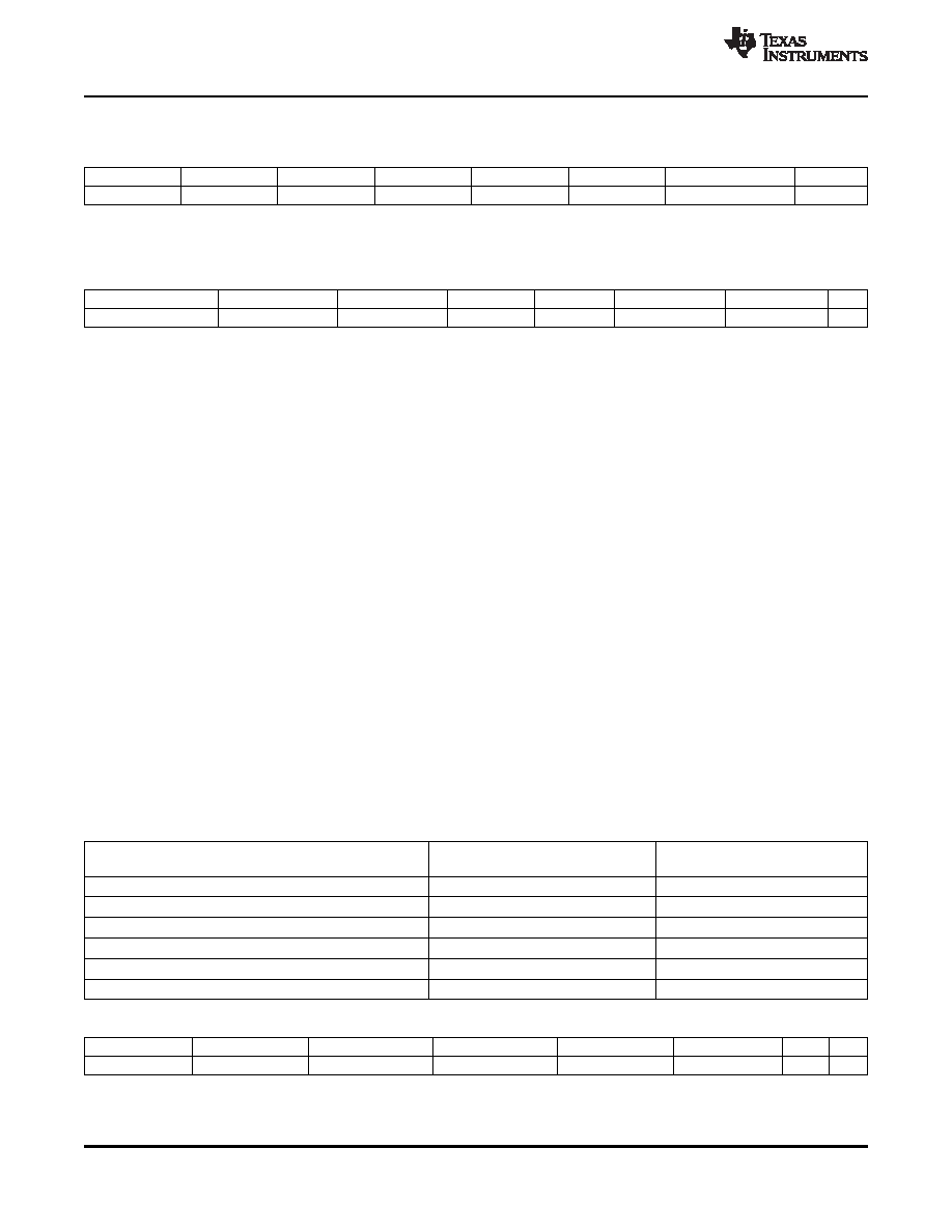
Register Name – CONFIG107 – Address 0x000, Default = 0x00
<7>
<6>
<5>
<4>
<3>
<2>
<1>
<0>
SOFTWARE_RESET
SOFTWARE_RESET:-Register bit to reset the device. Once set, the bit generates a reset pulse, which
resets all the register bits including itself.
Register Name – CONFIG108 – Address 0x207, Default = 0x00
<7>
<6>
<5>
<4>
<3>
<2>
<1>
<0>
REG_PDNFRM_REG
REG_PDN_FAST
REG_PDN_GBL
REG_PDNQ
REG_PDNI
REG_PDN_RX
REG_PDN_TX
REG_PDN_FRM_REG : Specifies whether the PDN control is through PIN or register bit. When cleared,
PDN pin is used as the master control.
For all the below power down modes to work, either set REG_PDN_FRM_REG or pull PDN pin to ‘High’.
REG_PDN_FAST : When REG_PDN_FRM_REG is low, this bit configures the PDN pin for fast
powerdown control. When REG_PDN_FRM_REG is high, this bit directly controls the fast powerdown
mode. When set, it power downs both transmitter and receiver but keeps certain blocks like reference
circuitry active. Also the Rx output clock is still active. This mode can be used where fast wake up times
are required.
REG_PDN_GBL : When REG_PDN_FRM_REG is low, this bit configures the PDN pin for global
powerdown control. When REG_PDN_FRM_REG is high, this bit directly controls the global powerdown
mode. When set, it powers down almost all circuitry inside the chip. Thus this mode can be used when
lowest power is desired. The wakeup times in this mode are much higher than in the fast powerdown
mode.
REG_PDNQ : Power downs Q channel of both transmitter and reciever.
REG_PDNI : Power down I channel of both transmitter and reciever.
REG_PDN_RX : Power downs reciever i.e both the ADC’s. Clock path is still active.
REG_PDN_TX : Power downs transmitter i.e both the DAC’s.
REG_PDN_FRM_REG has a similar role to play for the above modes (REG_PDNQ, REG_PDNI,
REG_PDN_RX, REG_PDN_TX). When REG_PDN_FRM_REG is low, it configures the PDN pin to the
function of the bit that is set. When REG_PDN_FRM_REG is high, the set bit directly controls the
described powerdown mode.
At 20 MHz Fs, the typical power consumption in different modes are as follows:
CURRENT ON 1.8 V SUPPLY
CURRENT ON 3 V SUPPLY
CONDITION
(mA)
Normal
63
58
Global Power down (REG_PDN_GBL = 1)
2.4
3
Fast power down (REG_PDN_FAST = 1)
25
13
Rx_power down (REG_PDN_RX = 1)
27
58
Tx power down (REG_PDN_TX = 1)
62
13
Both Rx and Tx (REG_PDN_TX = 1, REG_PDN_RX = 1)
25
13
Register Name – CONFIG109 – Address 0x208, Default = 0x00
<7>
<6>
<5>
<4>
<3>
<2>
<1>
<0>
REG_PDNI_TX
REG_PDNQ_TX
REG_PDNI_RX
REG_PDNQ_RX
MODE_LP_CMOS
REG_SINGLE
44
REGISTER DESCRIPTIONS
Copyright 2011–2012, Texas Instruments Incorporated
相關PDF資料 |
PDF描述 |
|---|---|
| ECE-V1EA100NP | CAP ALUM 10UF 25V 20% SMD |
| 0210491116 | CABLE JUMPER 1.25MM .305M 39POS |
| UPM1J270MED1TD | CAP ALUM 27UF 63V 20% RADIAL |
| RNF-100-1-1/4-RD-SP | HEAT SHRINK TUBING |
| RNF-100-1-1/4-BU-SP | HEAT SHRINK TUBING |
相關代理商/技術參數 |
參數描述 |
|---|---|
| AFE7222IRGC25 | 功能描述:射頻前端 Dual 12B,65MSPS ADC RoHS:否 制造商:Skyworks Solutions, Inc. 類型: 工作頻率:2.4 GHz, 5 GHz 最大數據速率:54 Mbps 噪聲系數: 工作電源電壓:3.3 V 電源電流:180 mA 最大工作溫度:+ 85 C 安裝風格:SMD/SMT 封裝 / 箱體:QFN-32 |
| AFE7222IRGCR | 功能描述:射頻前端 Dual 12B,65MSPS ADC RoHS:否 制造商:Skyworks Solutions, Inc. 類型: 工作頻率:2.4 GHz, 5 GHz 最大數據速率:54 Mbps 噪聲系數: 工作電源電壓:3.3 V 電源電流:180 mA 最大工作溫度:+ 85 C 安裝風格:SMD/SMT 封裝 / 箱體:QFN-32 |
| AFE7222IRGCT | 功能描述:射頻前端 Dual 12B,65MSPS ADC RoHS:否 制造商:Skyworks Solutions, Inc. 類型: 工作頻率:2.4 GHz, 5 GHz 最大數據速率:54 Mbps 噪聲系數: 工作電源電壓:3.3 V 電源電流:180 mA 最大工作溫度:+ 85 C 安裝風格:SMD/SMT 封裝 / 箱體:QFN-32 |
| AFE7225 | 制造商:TI 制造商全稱:Texas Instruments 功能描述:Analog Front End Wideband Mixed-Signal Transceiver |
| AFE7225EVM | 功能描述:射頻開發工具 AFE7225 Eval Mod RoHS:否 制造商:Taiyo Yuden 產品:Wireless Modules 類型:Wireless Audio 工具用于評估:WYSAAVDX7 頻率: 工作電源電壓:3.4 V to 5.5 V |
發布緊急采購,3分鐘左右您將得到回復。