欧美成人免费电影,国产欧美一区二区三区精品酒店,精品国产a毛片,色网在线免费观看
- 您現(xiàn)在的位置:買賣IC網(wǎng) > PDF目錄16699 > AFE7222EVM (Texas Instruments)EVAL MODULE FOR AFE7222 PDF資料下載
參數(shù)資料
| 型號(hào): | AFE7222EVM |
| 廠商: | Texas Instruments |
| 文件頁數(shù): | 92/106頁 |
| 文件大小: | 0K |
| 描述: | EVAL MODULE FOR AFE7222 |
| 標(biāo)準(zhǔn)包裝: | 1 |
| 主要目的: | 接口,模擬前端(AFE) |
| 嵌入式: | 否 |
| 已用 IC / 零件: | AFE7222 |
| 已供物品: | 板 |
| 其它名稱: | 296-30300 AFE7222EVM-ND |
第1頁第2頁第3頁第4頁第5頁第6頁第7頁第8頁第9頁第10頁第11頁第12頁第13頁第14頁第15頁第16頁第17頁第18頁第19頁第20頁第21頁第22頁第23頁第24頁第25頁第26頁第27頁第28頁第29頁第30頁第31頁第32頁第33頁第34頁第35頁第36頁第37頁第38頁第39頁第40頁第41頁第42頁第43頁第44頁第45頁第46頁第47頁第48頁第49頁第50頁第51頁第52頁第53頁第54頁第55頁第56頁第57頁第58頁第59頁第60頁第61頁第62頁第63頁第64頁第65頁第66頁第67頁第68頁第69頁第70頁第71頁第72頁第73頁第74頁第75頁第76頁第77頁第78頁第79頁第80頁第81頁第82頁第83頁第84頁第85頁第86頁第87頁第88頁第89頁第90頁第91頁當(dāng)前第92頁第93頁第94頁第95頁第96頁第97頁第98頁第99頁第100頁第101頁第102頁第103頁第104頁第105頁第106頁
ADC_DCLK
ADC_DATA
Ch A
Ch B
th
tsu
th
tsu
t
/6
CLK
ADC_DCLK
ADC_DATA
Ch A
Ch B
th
tsu
th
tsu
t
/3
CLK
SLOS711B – NOVEMBER 2011 – REVISED MARCH 2012
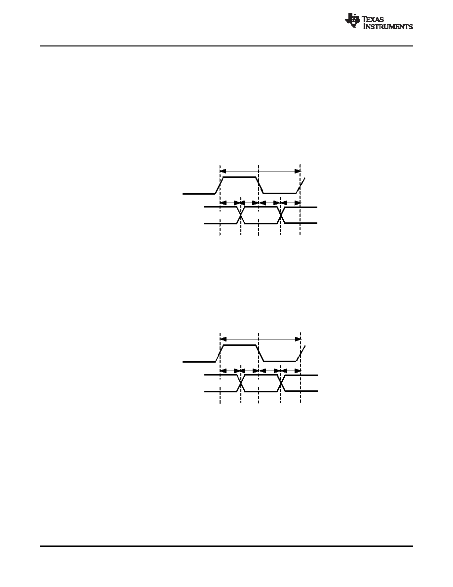
10.7 SERIAL LVDS ADC RX INTERFACE
Note: Set MASTER_OVERRIDE_RX bit to ‘1’ before entering RX LVDS interface.
The 12-bit ADC output data is serialized onto one or two LVDS pairs per ADC. ADCA and ADCB data
outputs can be quadrature data or two independent receive channels. Two serialization modes are
available.
1-Wire mode: 1 LVDS pair for the data from each ADC. It will operate in a DDR fashion serialized to a
frequency of 6x the pattern word rate. A frame clock (ADC_FCLKOUT) at the word rate and a bit clock
(ADC_DCLKOUT) at 6x. Example: 50MSPS 12-bit pattern will serialize to 300MHz on each LVDS pair,
frame clock of 50MHz and bit clock of 300MHz. Effective serial data rate is 600Mbps due to bit
transitions on rising and falling edge of bit clock.
A.
tCLK = Time period of ADC output frame clock.
B.
th is minimum hold time required at the AFE722x output.
C.
tsu is minimum setup time required at the AFE722x output.
Figure 10-9. RX 1-Wire Mode Timing Diagram
2-Wire mode, DDR clock: 2 LVDS pairs for the data from each ADC. It will operate in a DDR fashion
serialized to a frequency of 3x the pattern word rate. A frame clock (ADC_FCLKOUT) at half the word
rate and a bit clock (ADC_DCLKOUT) at 3x. Example: 50MSPS 12-bit pattern will serialize to 150MHz
on each LVDS pair, frame clock of 25MHz and bit clock of 150MHz. Effective serial data rate is
300Mbps on each LVDS pair due to bit transitions on rising and falling edge of bit clock.
A.
tCLK = Time period of ADC output frame clock.
B.
th is minimum hold time required at the AFE722x output.
C.
tsu is minimum setup time required at the AFE722x output.
Figure 10-10. RX 2-Wire Mode, DDR Clock Timing Diagram
2-Wire mode, SDR clock: 2 LVDS pairs for the data from each ADC. It will operate in a SDR fashion
serialized to a frequency of 6x the pattern word rate. A frame clock (ADC_FCLKOUT) at the word rate
and a bit clock (ADC_DCLKOUT) at 6x. Example: 50MSPS 12-bit pattern will serialize to 300MHz on
each LVDS pair, frame clock of 50MHz and bit clock of 300MHz. Effective serial data rate is 300Mbps
on each LVDS pair due to bit transitions on rising edge of bit clock.
86
DIGITAL INTERFACE
Copyright 2011–2012, Texas Instruments Incorporated
相關(guān)PDF資料 |
PDF描述 |
|---|---|
| ECE-V1EA100NP | CAP ALUM 10UF 25V 20% SMD |
| 0210491116 | CABLE JUMPER 1.25MM .305M 39POS |
| UPM1J270MED1TD | CAP ALUM 27UF 63V 20% RADIAL |
| RNF-100-1-1/4-RD-SP | HEAT SHRINK TUBING |
| RNF-100-1-1/4-BU-SP | HEAT SHRINK TUBING |
相關(guān)代理商/技術(shù)參數(shù) |
參數(shù)描述 |
|---|---|
| AFE7222IRGC25 | 功能描述:射頻前端 Dual 12B,65MSPS ADC RoHS:否 制造商:Skyworks Solutions, Inc. 類型: 工作頻率:2.4 GHz, 5 GHz 最大數(shù)據(jù)速率:54 Mbps 噪聲系數(shù): 工作電源電壓:3.3 V 電源電流:180 mA 最大工作溫度:+ 85 C 安裝風(fēng)格:SMD/SMT 封裝 / 箱體:QFN-32 |
| AFE7222IRGCR | 功能描述:射頻前端 Dual 12B,65MSPS ADC RoHS:否 制造商:Skyworks Solutions, Inc. 類型: 工作頻率:2.4 GHz, 5 GHz 最大數(shù)據(jù)速率:54 Mbps 噪聲系數(shù): 工作電源電壓:3.3 V 電源電流:180 mA 最大工作溫度:+ 85 C 安裝風(fēng)格:SMD/SMT 封裝 / 箱體:QFN-32 |
| AFE7222IRGCT | 功能描述:射頻前端 Dual 12B,65MSPS ADC RoHS:否 制造商:Skyworks Solutions, Inc. 類型: 工作頻率:2.4 GHz, 5 GHz 最大數(shù)據(jù)速率:54 Mbps 噪聲系數(shù): 工作電源電壓:3.3 V 電源電流:180 mA 最大工作溫度:+ 85 C 安裝風(fēng)格:SMD/SMT 封裝 / 箱體:QFN-32 |
| AFE7225 | 制造商:TI 制造商全稱:Texas Instruments 功能描述:Analog Front End Wideband Mixed-Signal Transceiver |
| AFE7225EVM | 功能描述:射頻開發(fā)工具 AFE7225 Eval Mod RoHS:否 制造商:Taiyo Yuden 產(chǎn)品:Wireless Modules 類型:Wireless Audio 工具用于評(píng)估:WYSAAVDX7 頻率: 工作電源電壓:3.4 V to 5.5 V |
發(fā)布緊急采購(gòu),3分鐘左右您將得到回復(fù)。